
Circuit Diagram
Index 1890
Digital multimeter circuit diagram composed of 8031 SCM and MAXl34
Published:2011/5/12 1:06:00 Author:Ecco | Keyword: Digital multimeter , SCM
Digital multimeter circuit diagram composed of 8031 SCM and MAXl344 3 / 4-bit integral A / D converter is shown as the chart.
(View)
View full Circuit Diagram | Comments | Reading(2969)
Interface circuit diagram between 8031 SCM and ICL7104 16-bit integrating A / D converter
Published:2011/5/12 1:04:00 Author:Ecco | Keyword: Interface , SCM , 16-bit , integrating , A / D converter
View full Circuit Diagram | Comments | Reading(829)
Digital power factor meter circuit diagram composed of ICL7107
Published:2011/5/12 1:17:00 Author:Ecco | Keyword: Digital , power factor meter
View full Circuit Diagram | Comments | Reading(8432)
BD200W emergency power supply circuit diagram
Published:2011/5/12 1:18:00 Author:Ecco | Keyword: emergency power supply
View full Circuit Diagram | Comments | Reading(674)
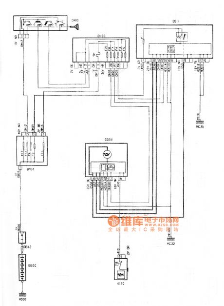
Peugeot Citroen 2.0L engine oil pressure circuit diagram
Published:2011/5/12 1:00:00 Author:Ecco | Keyword: Peugeot Citroen , 2.0L engine , oil pressure
View full Circuit Diagram | Comments | Reading(814)
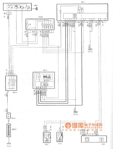
Dongfeng Peugeot Citroen Picasso 1.6L engine coolant temperature circuit diagram
Published:2011/5/12 1:01:00 Author:Ecco | Keyword: Dongfeng , Peugeot Citroen Picasso, 1.6L engine, coolant temperature
View full Circuit Diagram | Comments | Reading(708)
Dongfeng Peugeot Citroen Picasso 2.0L engine cooling system circuit diagram
Published:2011/5/12 0:56:00 Author:Ecco | Keyword: Dongfeng, Peugeot Citroen Picasso, 2.0L , engine , cooling system
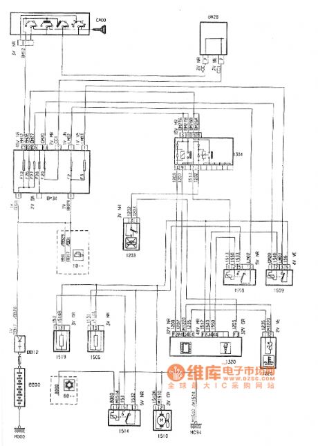
Dongfeng Peugeot Citroen Picasso 2.0L engine cooling system circuit diagram is shown as the chart.
(View)
View full Circuit Diagram | Comments | Reading(1477)
MN15287KEC31Single-chip Microcomputer Integrated Circuit
Published:2011/5/6 3:05:00 Author:Sharon | Keyword: Single-chip, Microcomputer, Integrated
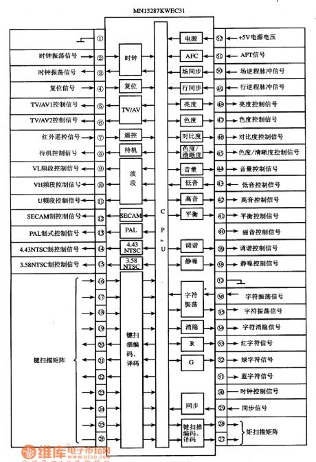
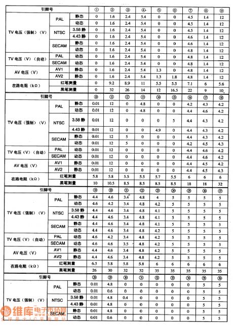
MN15287KEC31 is Panasonic's single-chip microcomputer integrated circuit, and is mainly used in a variety of large screen color TV of Toshiba, 1.Features:MN15287KWEC31 IC is usually used with monolithic memory integrated circuit MN12C2OlD to form a system control circuit of color television. It can control a variety of analog (brightness, color, contrast, volume control, bass and treble control, left and right channels balance control, etc.), TV / AV conversion, mode switch, tuning control, squelch control, etc. It also has a character display output circuit and the remote control signal processing circuit.2. Pin functions and dataMN15287KWEC31 IC is sealed in 52-pin dual packages, the internal circuit block diagram and pin functions and signal flow are shown in the figure, the operating parameters listed in Table.The measured data in the table is from Hong living (TA8611 + TA8759) movement on color TV.
(View)
View full Circuit Diagram | Comments | Reading(1096)
RMS Power Measurement Circuit`
Published:2011/5/9 22:16:00 Author:Sharon | Keyword: RMS, Power Measurement
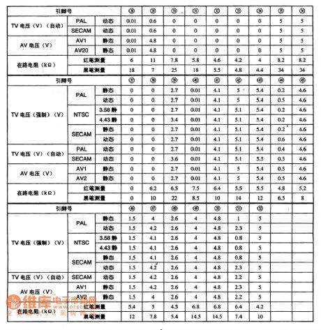
A true RMS power measurement circuit diagram is shown in below figure. The typical product corresponding to the circuit is the AD8361 monolithic RF RMS power detection IC. UI is for RF signal input, and Uo is for DC voltage output. Us termination is linked to+2.7 ~ +5.5 V power supply, and COM acts as public land. IREF is the work mode selective terminal, and PWDN is the sleep mode control terminal. FLTR is the filter terminal. Placing a capacitor between it and the Us side in parallel can reduce the filter cutoff frequency. SREF is the power control terminal. RF RMS voltage input from UI-end is UI, through square1 there generates a pulse current signal i proportional to UI2. The current signal gets through the square-law detector which is formed by the internal resistor R1 and capacitor C to obtain the mean square value of the voltage UI2, and then it is input to the error amplifier inverting.Squarer2 and the error amplifier can form a closed negative feedback circuit,whichwill addthe negative feedback signal into the error amplifier inverting input for temperature compensation. When the closed loop circuit reaches a steady state, the output voltage Uo (DC) is proportional to the input RMS power PIN. The relationship is: Uo = kPIN, where the k for the RMS / DC converter's output voltage sensitivity, AD8361 for k = 7.5mV/dBm.
This detection method has the following advantages: First, since the two squarers are identical, the change of range does not affect the conversion accuracy; second, when the ambient temperature changes, two squares can conduct mutual compensation, so that the output voltage is stable; third, the band of the used squarers are very wide, which isfrom DC to microwave frequencies.
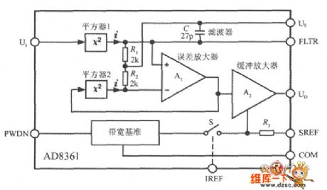
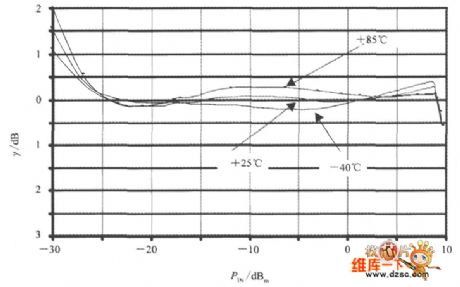
The RMS / DC detector Uo and PIN, γ the characteristic curve is shown below.
The figure shows that when input power is low, low temperature has a greater impact on output. AD8361 has internal temperature compensation circuit in itself. The characteristic curve after automatic compensation is shown below.
(View)
View full Circuit Diagram | Comments | Reading(1023)
Monolithic RF Power Measurement System AD8318 Typical Application Circuit
Published:2011/5/11 4:32:00 Author:Sharon | Keyword: Monolithic, RF power measurement, typical application
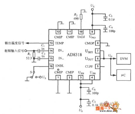
AD8318 typical application circuit is shown below. AD8318 is designed to measure RF power up to 8GHz. So, to maintain the insulation between the IN + and IN-pin and thefunctional unit circuit is essential. AD8318's positive power supply terminal UPSI and UPSO must take the same voltage. UPSI provides bias voltage for the input circuit andUPSO provides bias voltage for UOUT's low-noise output drive. Besides, there is still some independent public places within AD8318. CMOP is used as the public land of output drivers. All public places should be connected to PCB ground area of low impedance. The permitted supply voltage range is +4.5 ~ 5.5V. C3 ~ C6 is the power decoupling capacitors, which should be close to the power supply pin and ground. AD8318 applies AC coupled and single-ended input mode. When the input signal frequency is 1MHz ~ 8GHz, coupling capacitor (C1, c2) connected to the IN + and IN can use the 0402 1nF surface-mount-type ceramic capacitors, and coupling capacitors should be close to the IN +and IN-pin. External shunt resistor R1 (52.3Ω) is compatible with the IN + terminal, and can provide a 50Ω matching impedance of sufficient bandwidth. AD8318's output voltage can be directly sent to the digital voltmeter (DVM), and can also be sent to A / D converter's microcontroller (μC). To make AD8318 in working condition, ENBL end must be pulled through switch S to get a high electrical level(Us). When ENBL is grounded, AD8318 stays in sleep mode, and power supply current drops to 260μA. (View)
View full Circuit Diagram | Comments | Reading(984)
Monolithic RF Power Measurement System LT5504 Typical Application Circuit
Published:2011/5/11 4:30:00 Author:Sharon | Keyword: Monolithic, RF Power Measurement System, Typical Application
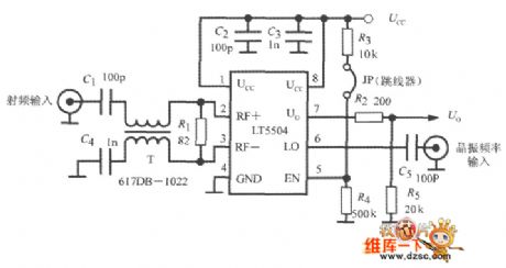
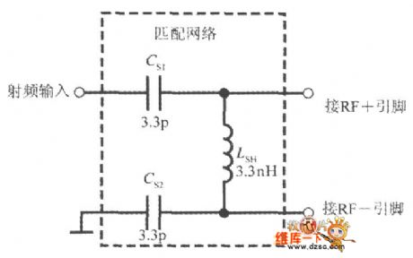
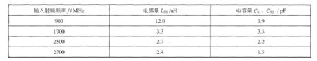

LT5504 typical application circuit is shown in the figure. RF signal passes through the coupling capacitor (C1) and 1:1 RF input transformer (T) to the LT5504 RF input. R1 is the shunt resistor. Crystal frequency is input to LO through terminal C5. Through the voltage divider R2 and R5, Uo end gets DC output voltage Uo. JP is the jumper. Since R4>> R3, when JP is connected, EN terminal raises the electrical level to make the circuit open. When JP is off,EN terminal drops the electrical level to close the circuit, and the chip gets into low power consumption mode. 1:1 RF input transformer's model number is 617DB-1022, which can also be replaced by the the narrow-band single-ended / differential conversion circuit constituted by three discrete components. The circuit is shownin the figureand the matching network's component values are listed in the table. According to different PCB design, the above-mentioned component values still need some adjustments.Voltage gain G of the narrow-band single-ended / differential conversion circuit is determined by below formula:
(View)
View full Circuit Diagram | Comments | Reading(758)
UV sensor schematic circuit
Published:2011/5/5 22:29:00 Author:Sharon | Keyword: UV sensor, schematic
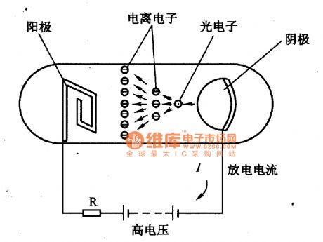
The figure is a schematic circuit of UV sensor. When UV sensor is coupled by voltage between the cathode and anode, and the UV radiation gets through the quartz glass tube on the cathode of the optical surface, because of the cathode material coated with electron emission, cathode will release photoelectrons.Influenced by the strong electric field, photoelectrons will be attracted to the anode, and high-speed movement of optoelectronics will lead to its collision with the gas molecules, which leads to ionization of them. Electron produced by ionization will further collide with gas molecules, and finally the cathode and the anode will be fulfilled by electrons and ions, causing the phenomenon of glow discharge, and the circuit generating a large current.When there is no ultraviolet radiation, there is no electrons and irons flow in the cathode and the anode , showing a very high level of impedance. (View)
View full Circuit Diagram | Comments | Reading(2925)
Monolithic RF Power Measurement System LTC5507 Typical Application Circuit
Published:2011/5/11 4:30:00 Author:Sharon | Keyword: Monolithic, RF Power Measurement, Typical Application
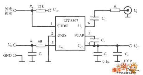
LTC5507 typical application circuit is shown in the figure. C1 is the RF input coupling capacitor, and C2 is the peak holding capacitor, both of which are ceramic capacitors and have less than 5Ω capacitance to reduce the ripple. C1 and C2's capacity depends on the minimum RF input frequency fmin (units of MHz), whose formula is: C1 = C21 ≥ (30fmin). Here, both C1 and C2's unit is μF. Considering the value of C2 will affect the conversion rate and bandwidth, generally C1 = C2. However, the capacity of C1 and C2 can not be set too big, otherwise it will exceed the minimum RF input frequency. Proper selection of the capacity of C1 and C2 can increase the conversion rate and the highest RF frequency AC characteristics. R3 is a pull-up resistor. When the SHDN is not floating, LTC5507 states in normal mode; when SHDN is grounded, LTC5507 turns to low-power consumption mode.
(View)
View full Circuit Diagram | Comments | Reading(1305)
pressure sensor application circuit
Published:2011/5/5 22:28:00 Author:Sharon | Keyword: pressure sensor, application
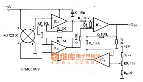
MPX2100 pressure sensor typical application circuit is as shown in the picture. RP1 in thepictureis used for full-scale adjustment, RP2 is used for zero adjustment when the pressure is zero. (View)
View full Circuit Diagram | Comments | Reading(2866)
piezoresistive pressure sensor circuit
Published:2011/5/5 22:28:00 Author:Sharon | Keyword: piezoresistive, pressure sensor,
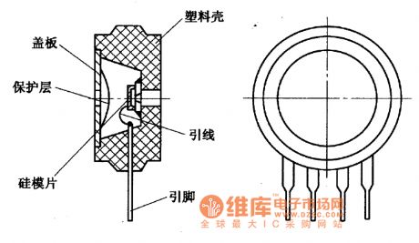
MPX205O and MPX2l00 type pressure sensor is a silicon piezoresistive pressure sensor, with the function of thermistor temperature compensation. The basic elements of its structure is as shown. (View)
View full Circuit Diagram | Comments | Reading(1363)
CL-YB-402 Force Sensor Scheme Circuit
Published:2011/5/6 3:03:00 Author:Sharon | Keyword: Force Sensor, Scheme
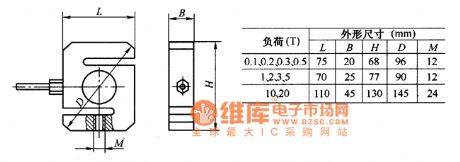
CL-YB-402 force sensor scheme circuithas thecharacteristics of overload and high precision, can be widely used in chemical, mining and other sectors in the truck and railroad track scale.Its dimensions are shown in the figure. (View)
View full Circuit Diagram | Comments | Reading(804)
NEC JC-140HM-type VGA Color Display Power Supply Circuit
Published:2011/5/9 22:25:00 Author:Sharon | Keyword: VGA, Color Display, Power Supply
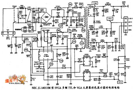
NEC JC-140HM-type VGA Color Display Power Supply Circuit is shown below:
(View)
View full Circuit Diagram | Comments | Reading(609)
GREAT WALL GW-600C-type V, SVGA Multi-frequency Display Power Supply Circuit
Published:2011/5/9 22:24:00 Author:Sharon | Keyword: V, SVGA, Multi-frequency Display, Power Supply
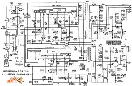
GREAT WALL GW-600C-type V, SVGA Multi-frequency Display Power Supply Circuit is shown in below figure:
(View)
View full Circuit Diagram | Comments | Reading(838)
Diode Detector Inputting Power circuit
Published:2011/5/9 22:10:00 Author:Sharon | Keyword: Diode Detector, Inputting Power
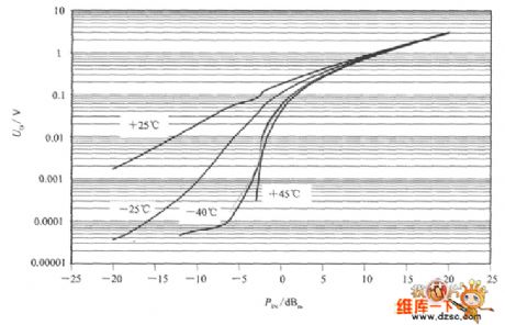
Diode detector inputting power circuit is shown in the figure. This is a simple half-wave rectifier and filter circuit. The circuit's total input resistance is 50Ω.VDis the rectifier, and Cis the filter capacitor. Input power PIN is rectified and filtered to output voltage Uo. The relation curve of Uo and the PIN at different ambient temperatures is shown below. The figure shows that only under the ambient temperature of +25 oC, Uo is approximately in linear relationship with the PIN; when the ambient temperature increases or decreases, Uo will reduce significantly.
(View)
View full Circuit Diagram | Comments | Reading(744)
Color Display EMC EM-1 Type Power Supply Circuit
Published:2011/5/9 22:24:00 Author:Sharon | Keyword: Color Display, Power supply
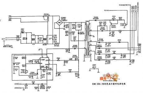
ColorDisplay EMC EM-1 Type Power Supply Circuit is shown in below figure:
(View)
View full Circuit Diagram | Comments | Reading(641)
| Pages:1890/2234 At 2018811882188318841885188618871888188918901891189218931894189518961897189818991900Under 20 |
Circuit Categories
power supply circuit
Amplifier Circuit
Basic Circuit
LED and Light Circuit
Sensor Circuit
Signal Processing
Electrical Equipment Circuit
Control Circuit
Remote Control Circuit
A/D-D/A Converter Circuit
Audio Circuit
Measuring and Test Circuit
Communication Circuit
Computer-Related Circuit
555 Circuit
Automotive Circuit
Repairing Circuit