
Circuit Diagram
Index 324
Ultrasonic beam barrier circuit
Published:2012/9/21 2:33:00 Author:Ecco | Keyword: Ultrasonic , beam barrier
This circuit generates inaudible ultrasound to make a barrier across the entry. At the moment the circuit detects a break in the sound barrier, it generates a loud alarm indicating the entry of a person. This can be used to protects the entry passages and helps to detect unauthorized entry of persons in protected areas. The circuit has two sections. An Ultrasound transmitter and a receiver. Both the circuits use 40 kHz Ultrasound transmitter (TX) and ultrasound receiver (RX) pair to transmit and receive the ultrasound.
The Transmitter section uses the ultrasound transmitter TX in conjunction with an emitter coupled oscillator comprising T1 and T2, both BC 548. The values of resistors and capacitors determine the oscillation at 40 kHz frequency which exactly matches with that of the transmitter.
Ultrasound Transmitter
Ultrasound Receiver
The receiver section has a 40 kHz ultrasound receiver RX which is connected to the base of T1.It is a common emitter amplifier which amplifies the signals received by the RX. The amplified signal available from the collector of T1 is coupled via C2 to the signal detector stage comprising T2 ,D1 and C3. When RX continuously receives the ultrasound from TX, T3 remains saturated and conducts. This keeps T4 output conduction since its base is at ground potential. When the ultrasound beam breaks, T3 turns off and T4 conducts. The piezo buzzer connected to the collector of T4 sounds the alarm. Red LED indicates the standby mode showing that the alarm system is active.
Range of the circuit
Range is a few meters .Properly align TX and RX on the opposite sides of the entry ,so that alarm will be off if the RX receives ultrasound from TX.
40kHz Ultrasound transmitter receiver pair
?
2 Responses to “Ultrasonic beam barrier circuit”
source: electroschematics.com
(View)
View full Circuit Diagram | Comments | Reading(1079)
Shadow Alarm Circuit
Published:2012/9/21 2:33:00 Author:Ecco | Keyword: Shadow Alarm
This shadow alarm circuit can sense a moving shadow in a confined area. It can be used to protect things from theft. When somebody approaches the unit, it will give a loud alarm to abort the attempt of theft. The circuit uses the light sensing property of the Photo diode.The circuit uses the light sensing property of the PIN Photodiode. The p-n junction of the photo diode gives light current when it is forward biased. IC1 is designed as a voltage comparator. Its non inverting input is connected to a potential divider R1 and VR. By adjusting VR, input current to pin3 can be set to a reference level. The inverting input of IC1 is connected to a photo diode. IC CA3130 is a 15 MHz BiMOS Operational amplifier with MOSFET inputs and bipolar output. The inputs contain MOSFET transistors to provide very high input impedance and very low input current as low as 10pA. It has high speed of performance and suitable for low input current applications.
CA3130A and CA3130 are op amps that combine the advantage of both CMOS and bipolar transistors. Gate-protected P-Channel MOSFET (PMOS) transistors are used in the input circuit to provide very-high-input impedance, very-low-input current and exceptional speed performance. The use of PMOS transistors in the input stage results in common-mode input-voltage capability down to 0.5V below the negative-supply terminal, an important attribute in single-supply applications.
A CMOS transistor-pair, capable of swinging the output voltage to within 10mV of either supply-voltage terminal (at very high values of load impedance), is employed as the output circuit.
The CA3130 Series circuits operate at supply voltages ranging from 5V to 16V, They can be phase compensated with a single external capacitor, and have terminals for adjustment of offset voltage for application requiring offset-null capability. Terminal provisions are also made to permit strobing of the output stage. The CA3130A offers superior input characteristics over those of the CA3130.
Normally in the light ( as set by VR) Photodiode gives voltage to pin2 of IC1.Since this voltage is higher than the voltage set by VR at pin3 ,output of IC1 remains low keeping LED and buzzer off. When a person approaches the photodiode, the shadow causes a reduction in current through the photodiode so that voltage at pin2 decreases below that of pin3. Output of IC1 then goes high and Buzzer sounds.
NoteThe circuit triggers when the light intensity changes without a shadow. It is better to keep the unit in a place where constant light is available
Shadow Alarm Circuit diagram
?
68 Responses to “Shadow Alarm Circuit”
source: electroschematics.com (View)
View full Circuit Diagram | Comments | Reading(1156)
Outdoor Garden Solar Lights circuit
Published:2012/9/20 21:06:00 Author:Ecco | Keyword: Outdoor Garden, Solar Lights
This Outdoor LED Solar Garden Lights project is a hobby circuit of an automatic garden light using a LDR and 6V/5W solar panel. During day time, the internal rechargeable 6 Volt SLA battery receives charging current from the connected solar panel through polariy protection diode D9 and current limiting resistor R10. If ambient light is normal, transistor T1 is reverse biased by IC1 (LM555).
LED Solar Lights Circuit Schematic
Here IC1 is wired as a medium current inverting line driver, switched by an encapsulated light detector (10mm LDR). Multi-turn trimpot P1 sets the detection sensitivity. When ambient light dims,transistor T1 turns on to drive the white LED string (D1-D8). Now this lamp load at the output of T1 energises. Resistors R1-R8 limits the operating current of the LEDs. When the ambient light level restores, circuit returns to its idle state and light(s) switched off by the circuit.Assemble the Outdoor Solar Lights circuit on a general purpose PCB and enclose the whole assembly in a transparent plastic box. Drill suitable holes on the top of the encloure to mount the mini solar panel (SP1) and the light sensor (LDR), and in front for fitting power switch (S1) and the sensitivity controller (P1).Fix the battery inside the cabinet using a double-sided glue tape/pad. Finally, the LDR should not be mounted to receive direct sunlight. It must be mounted at the top of the enclosure, pointing to the sky say southwards. This circuit is very simple. So interested and experienced hobbyists can alter/modify the whole circuit as per their own ideas without any difficulty (Just try a 6V relay with T1 to drive more number of LED strings)?
27 Responses to “Outdoor Garden Solar Lights circuit”
Source: electroschematics.com (View)
View full Circuit Diagram | Comments | Reading(3732)
Earth Fault Indicator circuit
Published:2012/9/20 21:05:00 Author:Ecco | Keyword: Earth Fault, Indicator
This circuit indicates the integrity of wiring connections. It shows all the mains connections – Phase, Neutral and Earth connections – are intact or not. The circuit is too small and can be housed in a three pin plug case.
Earth Fault Indication Circuit Diagram
The circuit is directly connected to mains to monitor the status of the connections. Earth connection is a must in domestic wiring to bleed current to the earth if the metal body of a device is accidentally touched with the phase line. This circuit indicates
1. Red and Green LEDs ON Phase, Neutral and Earth OK2. Red and Green LEDs OFF Phase or Neutral Break / Power failure3. Red LED ON Phase and Neutral OK3. Green LED OFF Earth line break
The circuit gets power supply through C1 and R3. AC Capacitor C1 reduces the high volt AC to a safer level through capacitive rectance. Resistor R3 limits the inrush current and R4 gives discharge path for the stored current in C1 when the circuit is unplugged. Zener diode ZD regulates the voltage to a safer level to protect T1 when it is off. Voltage across ZD will be a square wave by the working of C1 and the voltage level depends on the breakdown value of zener (9 volts). When a potential of 230 volt is present between the phase and neutral lines, T1 turns on during the negative half cycle of AC and Green LED lights indicating that Earth connection is intact. This is because the base of T1 will be biased by the potential difference between the phase line and earth. If the earth connection is not intact, T1 will not get base bias and it remains off. Red LED lights during the positive half cycle of AC due to the potential difference between the phase and neutral lines.Enclose the circuit in a 3 pin plug and connect points A, B and C to the phase, neutral and earth pins respectively. Plug it into the 3 pin socket to test the wiring.
Warning The circuit is kept at mains lethal potential. Do not touch any parts to avoid lethal shock. Do not construct this circuit unless you are experienced in handling High volt AC.?
16 Responses to “Earth Fault Indicator circuit”
Source: electroschematics.com
(View)
View full Circuit Diagram | Comments | Reading(1700)
Small FM Receiver Circuit
Published:2012/9/20 21:04:00 Author:Ecco | Keyword: Small , FM Receiver
This is the most simple fm radio receiver with good performances that works great even if the sensitivity is not too high. The working principle of this fm receiver may seem a little unusual. It is made of an oscillator (T2 and T3) that is synchronized with the received frequency of T1. This transistor works as a broadband preamplifier in VHF range.The oscillator is adjusted between 87 … 108 MHz with C5. Because of the synchronization, the oscillator output will have the same frequency deviation as the received signal from the fm antenna. This deviations are caused by the broadcasted audio informations. The frequency modulated signal show up on P1 + R5. Low pass filter R6/C6 extracts the audio signal and then is amplifier by T4 … T6 and transmitted at the output through C9 capacitor.
FM Receiver Circuit Diagram
The coil details are presented in the fm receiver circuit diagram. The radio receiver is adjusted on different stations with the help of C5. P1 potentiometer is adjusted untill the best reception is obtained. If we attach an audio amplifier and a speaker then this fm receiver can be made very compact as a pocket radio.?
72 Responses to “Small FM Receiver Circuit”
(View)
View full Circuit Diagram | Comments | Reading(1263)
27MHz CB receiver circuit
Published:2012/9/20 21:04:00 Author:Ecco | Keyword: 27MHz , CB receiver

This is a simple 27MHz FM-CB receiver circuit built with TCA440 for listening CB ( citizen’s band ) transmissions with FM (frequency modulation). The selection is made with ceramic filters. This 27 MHz receiver works with an intermediary frequency of 455 kHz. The input filter is 27 MF type, so we obtain an acceptable attenuation of the mirroring frequency.
CB 27MHz Receiver Circuit Schematic
Because the intermediary frequency filter is used without adapting transformer, the selection is at 40 dB. Because of the noise in the transmission pauses, the CB receiver circuit has a squelch circuit which reacts at 4.5 kHz domain noise.?
6 Responses to “27MHz CB receiver circuit”
Source: electroschematics.com
(View)
View full Circuit Diagram | Comments | Reading(3691)
Fatigue Testing circuit
Published:2012/9/20 21:03:00 Author:Ecco | Keyword: Fatigue Testing
This fatigue testing circuit is very simple and easy to build and will determine how tired a person is. It has been discovered that the highest light frequency that a human can detect is negatively influenced by his fatigue. This circuit is based on 555 timer that is connected here as an astable multivibrator. Its output is connected to a LED that is flashing with a certain frequency.With P1 potentiometer that frequency can be adjusted between 20 and 50 Hz. The highest flashing frequency the humans can detect is somewhere between 30 and 40 flash per second but a test made by us in a early morning produced some questions like: “What LED?”.
Fatigue Tester Circuit Diagram
To make a reliable fatigue test you must adjust P1 when you are not tired. So, adjust P1 untill you just start not seeing the LED light. Leave it like that and then power up the circuit when you are tired and you will notice that the LED light has gone .
Because of the fatigue tester circuit nature, there is no wonder it has a small current consumption of just 25 mA so you can powered it up from a 9 V battery. Do not consider this to be equal to fatigue testers found on the market.?
No Responses to “Fatigue Testing circuit”
(View)
View full Circuit Diagram | Comments | Reading(1135)
Audio Mixer with one transistor
Published:2012/9/20 20:59:00 Author:Ecco | Keyword: Audio Mixer , one transistor
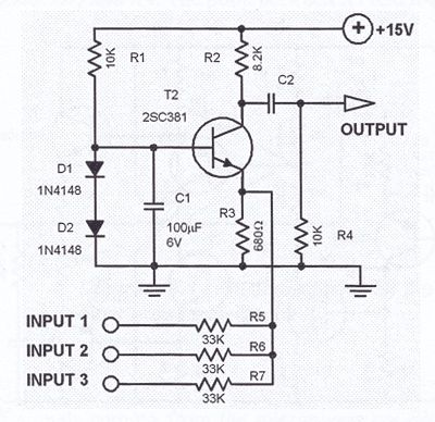
This one transistor audio mixer is used in an amplifier circuit design with base driven transistor and with its emitter being current controlled, most of the driving current flows through the collector away. Using the values in the audio mixer circuit shown in the diagram, the collector current will be about 1 mA. At 15 volts power supply, the input resistors should be 33K. Additional input lines can be connected to the emitter line. Each added input must be series limited by the 33K resistor.
Audio mixer circuit diagram
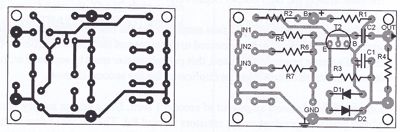
Mixer PCB Layout
(View)
View full Circuit Diagram | Comments | Reading(3445)
DC Electronic Fuse
Published:2012/9/20 20:58:00 Author:Ecco | Keyword: DC Electronic Fuse
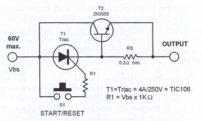
This DC electronic fuse never needs to be replaced. It can be repaired with just a single press of the start/reset button S1. Once S1 is pressed, the thyristor T1 triggers and the current flows to the consumer load through T1 and resistor RS. Even after releasing the start button, the current continue to flow as long as the current’s value does not sink below a certain level.
Electronic DC fuse circuit diagram
The current flowing through the thyristor T1 will sink below the holding level when the current is rerouted through the transistor T2 2N3055. T2 and RS are built into the electronic fuse circuit for this purpose. If the voltage drop at RS exceeds above base-emitter-diode trigger voltage of the T2, the transistor conducts thereby bypassing the thyristor. The resistance value of RS must be at least 0.2 W. It must be dimensioned that the product of RS multiplied by the fuse current value equals to 0.7 volts.
Once T2 bypasses the T1, the current flowing through the thyristor sinks below the holding level and the T1 shuts off. This in turn causes the voltage drop at resistor RS to sink below the base-emitter trigger voltage of T2 and the transistor shuts off. The end result is the shutting off of the whole circuit. The DC fuse can be reactivated by pressing the start/reset button.
The value of resistor R1 is dependent on the supply voltage. Multiply the supply voltage with 1 KW to get the value of R1. Connect the dc electronic fuse circuit to the PLUS line of the consumer load. THe coltage drop at the circuit is less than 1 volt.
DC fuse PCB layout
?
3 Responses to “DC Electronic Fuse”
(View)
View full Circuit Diagram | Comments | Reading(1836)
Blinker circuit
Published:2012/9/20 20:58:00 Author:Ecco | Keyword: Blinker
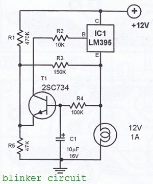
The blinker circuit design is made using the LM395 IC. This IC is a short-circuit proof power transistor with special characteristics. This is sometimes called a “super transistor”. LM395 is used in this circuit as an alarm blinker for cars.
12 volts Blinker circuit diagram
The blink frequency is determined by the R4/C1 combination which is dimensioned to give approximately one blink per second. To achieve lower frequencies, increase the value of C1. To achieve faster blink freq decrease the value of C1. The circuit cand drive 12 volts lamps. The maximum power delivered is 12 watts. The power transistor T1 must be heatsinked. Two PCB desing are available: one for TO-3 package and one for the TO-220 package.
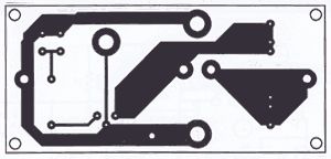
LM395 TO-3 Blinker PCB Layout
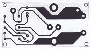
LM395 TO-220 Blinker PCB desing
?
One Response to “Blinker circuit”
(View)
View full Circuit Diagram | Comments | Reading(2329)
Speaker balance indicator circuit
Published:2012/9/20 20:58:00 Author:Ecco | Keyword: Speaker balance , indicator
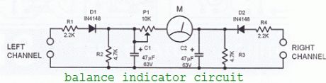
You may use this speaker balance calibrating circuit when using a stereo amplifier, there are many possible mechanical problems that may influence the amplifier’s output performance. The usual culprit is the mechanical potentiometers which are not rarely unsync in their stereo resistance pads. This results to unbalanced volume levels on the audio channels. Most good stereo units have a balance control to compensate for this imbalance.In using this balance indicator circuit, its left and right input channels are connected to the corresponding speaker outputs of the amplifier. Identical signals are then fed to the amplifier’s stereo inputs. When a signal of exactly the same amplitude is coming out from both speaker outputs, the meter M of the speaker balance circuit will stay at its zero setting. The meter M is a type with a zero setting at the middle of the scale. This enables one to see at first glance when one channel is louder than the other channel
Calibrating the speaker balance indicator circuit
Inject a signal in one channel and set the amplifier’s volume to maximum.While doing this, turn the potentiometer P1 until the meter swings to end of the scale in the direction of the channel.
Balance indicator circuit diagram
(View)
View full Circuit Diagram | Comments | Reading(1534)
Infrared detector with PID20
Published:2012/9/20 20:58:00 Author:Ecco | Keyword: Infrared detector
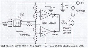
This infrared detector circuit uses a passive IR-detector component PID20. It converts heat radiation into electrical impulses. The output voltage of the PID20 increases when an object comes close to it, this object must be warmer than the surroundings.The voltage changes at the output of the IR sensor are sensed by the comparators IC2a and IC2b. Once the sensor detects an object (independent of the object’s actual temperature), one of the comparators will turn on the transistor T1. This transistor then closes the relay connected to it. A separate transistor for each comparator can be used so that the sensor will be able to determine whether the object is warmer or colder than the surroundings. The IR detector circuit consumes around 1 mA and the sensor consumes 0.2 mA.
IR detector circuit diagram
Source: electroschematics.com?
One Response to “Infrared detector with PID20”
(View)
View full Circuit Diagram | Comments | Reading(1958)
Small FM Radio Circuit
Published:2012/9/20 20:56:00 Author:Ecco | Keyword: Small FM Radio
Perhaps this is one of the simplest and smallest FM radio receiver that can receive the FM stations available locally. Its simple design makes it ideal for a pocket sized FM receiver. The output of the receiver drives a head phone.
Tiny FM Radio Receiver Circuit Schematic
The circuit works off a small 4.5 volt battery or two 3.6 volt Lithium button cells.The fm receiver section has two RF transistors T1 and T2 to detect the Frequency Modulated signals. Coil L1 and the trimmer capacito form the tuned tank circuit to tune the receiver to the best FM station with strong signals. The signals are capacitor coupled through C2.
10K preset VR controls the volume to the input of the amplifier. IC1 is the micro power audio amplifier that works between 4.5 to 12 volts DC. The amplified sound can be heard through the low impedance head phone or small Mylar speakers.
FM radio coilCoil is the important part of the FM tuner. It is made up of 18 SWG enameled copper wire. Wind 4 turns on a ball pen to get 0.5 cm inner diameter. Remove the enamel from the tip of the wire and solder tightly in the PCB. Trimmer and coil should be soldered very closely. Adjust the spacing of the coil winding if necessary to get the station clearly. Assemble all the receiver components as close as possible to get better result.
Pinout of BF494 and LM386
?
33 Responses to “Small FM Radio Circuit”
Source: electroschematics.com
(View)
View full Circuit Diagram | Comments | Reading(2897)
Aquarium Led Lighting circuit
Published:2012/9/20 20:55:00 Author:Ecco | Keyword: Aquarium , Led Lighting
This colorful back led aquarium lights gives natural appearance to the Aquarium tank. The Aquarium Led Lighting circuit automatically turns on at sunset and gives changing White, Blue and Green color display to make the aquarium attractive. In the morning the aquarium led light turns off.The aquarium led light circuit uses LDR as light sensor for automatic switching of the circuit. During day time LDR has very low resistance so that IC1 remains stand by. In the night, LDR offers high resistance and the reset pin 12 of IC1 becomes low. This activates IC1. CD4060 is a binary counter with ten outputs. The outputs of IC become high one by one based on the frequency of counting determined by C1, R1 andR2. In the aquarium led light circuit, strings of LEDs are connected to the collector of switching transistors T1 through T3.
When the IC triggers, oscillations starts and the output Q6 turns on after 5 minutes and stays on for another five minutes to light Blue LEDs. After 10 minutes Q7 output becomes high and Green LED turns on. They remain on for 10 minutes. After half time, Blue LEDs also turn on. This gives a mixture of Blue and Green colors for 5 minutes. After 20 minutes Q9 output becomes high and White LEDs turn on. They remain on for 20 minutes. During this period, Blue-White, Green-White and Blue-Green-White color combinations develop. This gives beautiful color display to the background of the Aquarium tank.
Aquarium LED Lights Circuit diagram
Note: Keep LDR in a position at which it illuminates in day light but dark in night.?
30 Responses to “Aquarium Led Lighting circuit”
Source: electroschematics.com
(View)
View full Circuit Diagram | Comments | Reading(2179)
Telephone Status Indicator circuit
Published:2012/9/20 20:55:00 Author:Ecco | Keyword: Telephone Status, Indicator
This simple circuit tells you about the status of phone such as Line OK, Dialing and Call attended. It also has a lock facility to block outgoing calls keeping the incoming calls as usual. This prevents misuse of telephone. The circuit uses only a few components to do all these jobs. The circuit is directly connected to the telephone lines and no power supply is needed. In the On Hook state, the telephone lines have around 48 volts which reduces to 12 volts in Off Hook state. More over the line polarity changes during dialing and two way speech. Capacitors C1 reduce the line voltage to a safer level for the operation of LEDs. When the phone is Off Hook, Red LED lights to indicate that the lines are OK. When a call is dialed, Red LED blinks to indicate the dialing status. When the remote person attends the call, Green LED lights indicating that the call is attended.
Telephone Status Indicator Circuit diagram
A simple Toggle switch is provided as Lock. It can be replaced with an electrical lock with key. When the switch is in Off position, outgoing calls will be blocked but the telephone receives incoming calls as usual.
Electrical Lock
?
2 Responses to “Telephone Status Indicator circuit”
Source: electroschematics.com
(View)
View full Circuit Diagram | Comments | Reading(1336)
LED Component Tester with Torch
Published:2012/9/20 20:55:00 Author:Ecco | Keyword: LED Component Tester , Torch
Here is a simple tester for Hobbyists. This LED Component tester can test the integrity of electronic components from resistors to ICs before soldering. It reduces the job of testing the components using multimeter. The tester gives LED indications about the Good or Bad conditions of the components. A White LED torch is added to verify the value of the components if light is not sufficient.The circuit layout is straight forward. Two bipolar NPN transistors are used to drive two LEDs based on their base bias. When the tester is switched on through S2, Red LED lights because T2 gets base bias through R2. At the same time, Green LED remains off because the base of T1 is floating .
When a component is placed between the Probes, electrical continuity establishes and T1 gets base current through R1. When T1 conducts, Green LED turns on and Red LED turns off since the base of T2 is grounded when T1 conducts. This indicates that the component under test is good. In short Green LED lights only when a good component is connected to the probes. If the component is bad, probes will not get electrical continuity and T1 remains off. In this state only Red LED light indicating that the component is bad. Test procedure is given below.
LED Component Tester Circuit diagram
Test Procedure
1. PolarityConnect Red probe to positive track of circuit board and Black probe to test point. Circuit board under test should be ONGreen LED ON – Positive supply. Green LED OFF and Red LED ON – Negative supply or No power
2. ContinuityConnect both Red and Black probes across the test pointsGreen LED ON- Continuity. Green LED OFF and Red LED ON- No continuity
3. Resistor. 1 Ohm to 500KConnect Red and Black probes on either side of ResistorGreen LED ON- Resistor OK. Green LED OFF and Red LED ON-Resistor burned
4. Capacitor ElectrolyticRed probe to positive and Black probe to negative of capacitorGreen LED ON and gradually fades and then Red ON- Capacitor Good. Red LED always ON- Capacitor bad
5. Capacitor DiscSame as above.Probes can be connected either way round
6. LED, Diodes, Photodiodes, Infrared diodesRed probe to Anode and Black probe to CathodeGreen LED ON – Good diode and LED. Green LED OFF and Red LED ON- Diode or LED badChange the direction of Probes. If the Green LED ON diode or LED is Open
7. LDRRed and Black probes at the leads of LDRGreen LED ON and Red LED OFF. Mask with hand. Green LED turns OFF-LDR good
Probes with Crocodile Clips
?
One Response to “LED Component Tester with Torch”
Source: electroschematics.com
(View)
View full Circuit Diagram | Comments | Reading(1389)
Power Supply Regulation
Published:2012/9/20 20:54:00 Author:Ecco | Keyword: Power Supply , Regulation
Regulated power supply is necessary in some electronic circuits especially in Amplifier circuits. Poorly regulated power may cause buzzing and unwanted noise in RF and amplifier circuits. There are two methods to get regulated power supply. The most common and simple one is Zener regulated power supply. A Regulator IC of 78 XX series or Variable regulator LM317 can also be used but it may increase the cost and size of the power supply circuit. Here explains the theory behind Zener regulation. Zener Regulation is used to hold the output voltage steady, irrespective of the changes in input voltage. Zener is a sophisticated semiconductor diode. It conducts only when its breakdown voltage reaches. Zener value represents the voltage it gives. But to get easy breakdown of Zener, the input voltage must be 1-2 volts higher than that of the Zener voltage.
Low current Zener Regulation
Fig.1 shows the voltage regulation using a Zener diode.10 V input is given to a 5.6V Zener. Zener requires a minimum 5 mA current to maintain its action. This current is maintained by the series resistor R connected in series with the Zener. The value of R is important to allow at least 5 mA current for the Zener even if the load draws more current.
Zener Regulation Circuits
In the Fig.1 Imax is the current through the load. It should be maximum 250mA.
Iz is the current passing through the Zener to maintain its action
I max + Iz is the current passing through the resistor R.
Vz is the voltage across the Zener
Using these parameters, the value of the resistor R is determined using the formula
R = (Vin-Vz) / (Imax+Iz)
That is (10-5.6) / (0.25A+0.005A) = 4.40 / 0.26 = 16 Ohms. The nearest value is 18 Ohms.
Power rating of the Zener should be enough to withstand current through the Zener in no load condition.
Power rating of the Zener is calculated using the formula
P = (I max + Iz) x Vz = P = (0.25 A+0.005A) X 5.6 = 1.4 Watts. Select a Zener with more than 1.5 W rating, if the load current is 250 mA.
Rating of the resistor R is also important to handle the load current as well as the Zener current.
Current through R is I max + I z and voltage through R is Vin – Vz
So Power dissipation in R is
P= (Imax+Iz) x (Vin-Vz) = (0.25+0.005) x 10-5.6) = 1.14 W. So a 2 watt resistor is required as R if the load current is 250 mA or 0.25 A.
High Current Regulation
The circuit shown in Fig.1can be used only if the load current is less than 250 mA. If the load requires more current, say as in battery charges, transistor based Zener regulation is necessary. Fig.2 shows how a series transistor is used in combination with a Zener to give a High current voltage regulated circuit. T1 is connected as an Emitter follower. It should be either a medium power transistor like BD 139 or TIP 122 if current is less than 1A or power transistor like 2N 3055 if current is very high. Zener voltage Vz is 0.7 V (biasing voltage of T1) more than the required output. R s
Source: electroschematics.com (View)
View full Circuit Diagram | Comments | Reading(1249)
Low cost Pilot Lamp
Published:2012/9/20 20:53:00 Author:Ecco | Keyword: Low cost , Pilot Lamp
This is the simple way to connect an LED in the Mains to use it as a pilot lamp. It takes little current compared to a neon lamp. It can power low efficiency as well as high efficiency LEDs including White and Blue LEDs.The pilot lamp circuit is straight forward. A rectifying diode IN4007 (1A) is connected in series with the phase line. The rectified voltage is reduced to low volt by the resistor R1. Capacitor C1 filters some ripples and act as a buffer to provide continuous supply to the LED as the AC waveform swings. Resistor R2 determines the brightness of LED. With 1.5 K resistor, adequate brightness can be obtained.
Low cost Pilot Lamp Circuit
Important Note The pilor lamp circuit is directly connected to mains and hence at lethal potential. Do not touch or troubleshoot when it is connected to mains.?
8 Responses to “Low cost Pilot Lamp”
Source: electroschematics.com (View)
View full Circuit Diagram | Comments | Reading(1236)
Tricky Charger circuit
Published:2012/9/20 20:53:00 Author:Ecco | Keyword: Tricky Charger
Here is a crude but efficient tricky charger for Lead Acid Battery. It uses a 12 volt car bulb as current regulator and charge status indicator. The brightness of the bulb indicates how much charge is flowing into the battery. When the battery becomes fully charged, lamp turns off. If the lamp is staying on with full brightness for more than 30 minutes, it indicates that the battery is dead and is not accepting charge.Charging current is obtained from a 15-0-15 volt secondary 2 Ampere step down transformer. Diodes D1 and D2 are rectifiers which can handle 3 ampere current. In order to give “Dirty DC” for charging, a low value filtering capacitor C1 is used. So that the DC voltage will have some ripples which is necessary for better charging of lead acid battery.
Tricky Charger Circuit diagram
The trick of the lamp is interesting. A 12 volt car tail lamp bulb is used in the circuit. It is connected in series with the positive output rail so that current flows through the bulb into the positive terminal of the battery. From the positive terminal, current passes through the battery chemistry into the negative terminal and then returns into the transformer. So the current flowing through the bulb depends on how much charge is using by the battery. When the charger is connected to the battery, the lamp turns on only if the battery requires charging current. OFF state of the bulb indicates that the battery is dead. If the battery holds some charge, bulb will turns on. If the battery is partially discharged and holding 50% charge, bulb will light brightly when the charger turns on. Then the brightness gradually reduces and finally the filament appears as a red hot line. This indicates that the battery is fully charged. The bulb also restricts the flow of current like a resistor.?
7 Responses to “Tricky Charger circuit”
Source: electroschematics.com (View)
View full Circuit Diagram | Comments | Reading(1917)
Water sensor alarm
Published:2012/9/20 20:52:00 Author:Ecco | Keyword: Water sensor, alarm

This small water sensor alarm circuit makes a loud warning sound when a humidity sensor detects a quantity of water. This circuit assembly is an application of low power comparator LM1801 made by National Semiconductor. The reference voltage for the integrated circuit is fixed with the help of R2.When pin 4 of the LM1801 voltage exceeds preset threshold, because the moisture sensor noticed a smaller or larger chip will command the active piezoelectric buzzer with a current of over 24 mA.
In the surveillance state, the water sensor alarm circuit has a current consumption of 10 microAmps so you can use a 9V battery for almost one year. We can connect many sensors simultaneously.
Water sensor alarm circuit diagram
?
3 Responses to “Water sensor alarm”
Source: electroschematics.com (View)
View full Circuit Diagram | Comments | Reading(3112)
| Pages:324/2234 At 20321322323324325326327328329330331332333334335336337338339340Under 20 |
Circuit Categories
power supply circuit
Amplifier Circuit
Basic Circuit
LED and Light Circuit
Sensor Circuit
Signal Processing
Electrical Equipment Circuit
Control Circuit
Remote Control Circuit
A/D-D/A Converter Circuit
Audio Circuit
Measuring and Test Circuit
Communication Circuit
Computer-Related Circuit
555 Circuit
Automotive Circuit
Repairing Circuit