
Circuit Diagram
Index 774
FET_PINCHOFF_VOLTAGE
Published:2009/7/17 2:58:00 Author:Jessie
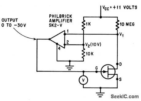
Measures gate-source voltage while drain current is below 0.1 microamp, to give value that matches pinchoff voltage of let.-B. R. Smith and I. C. Chase, Matching Cote Potential to FET Pinchoff Voltage, Electronics, 38:16, p 81. (View)
View full Circuit Diagram | Comments | Reading(754)
Operational_integrator
Published:2009/7/17 2:57:00 Author:Jessie
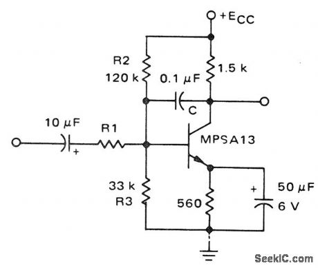
Operational integrator. Two cascaded 2N3904s can replace the MPSA 13 (courtesy Motorola Semiconductor Products Inc.). (View)
View full Circuit Diagram | Comments | Reading(934)
STOPPING_PADDLE_BOUNCE
Published:2009/7/11 4:01:00 Author:May

Simple circuit prevents generation of erroneous dots by paddle contact bounce in keyers having dot memory. Uses 74121 mono MVBR and 7432 AND gate. Output of 74121 stays low if paddle is not in use or if dots or dashes are being sent. Release of dash paddle makes 74121 transmit high-level pulse to AND gate, long enough to block dot caused by bounce. Suitable only for keyers using +5 V.-B. Locher, Keyer Modifi-cation, Ham Radio, Aug. 1976, p 80. (View)
View full Circuit Diagram | Comments | Reading(1592)
VAVUM_TUBE_SW_RECEIVER
Published:2009/7/17 2:57:00 Author:Jessie
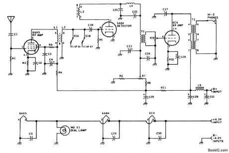
This vacuum-tube receiver covers from 9.4 to 22 MHz and is of interest to those hobbyists who wish to experiment with vacuum-tube circuitry. (View)
View full Circuit Diagram | Comments | Reading(1695)
TWO_TIMER_KEYER
Published:2009/7/11 4:00:00 Author:May
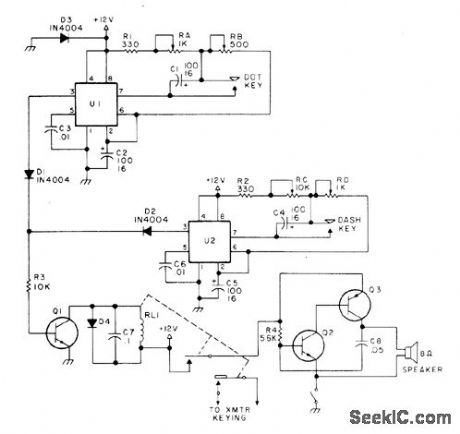
Characters are self-completing and fully adjustable as to speed and length of character. When dot key is closed, NE555 timer U1 becomes astable MVBR with speed determined by F1B and dot duration by RA Identical timer U2 provides longercharacter lengths for dashes. All diodes are 1N4004 or equivalent 400 V PIV at 1 A. Q1 and Q2 are 2N2222, Q3 is 2N5964, and RL1 is 12-V reed relay. Capacitor values are in microfarads. All pots are linear. Power is not regulated.-A.Ring, Build the World's Simplest Keyer, 73 Magazine, May 1977, p 46-47. (View)
View full Circuit Diagram | Comments | Reading(881)
PROTON_PRECESSION_MAGNETOMETER
Published:2009/7/17 2:57:00 Author:Jessie
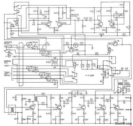
Used in Vanguard III satellite for magnetic field measurements at altitudes of 510 to 3,750 km.-D. Mansir, Magnetic Measurements in Space, Electronics, 33:32, p 47-51. (View)
View full Circuit Diagram | Comments | Reading(985)
Logarithmic_amplifier_using_an_MC1556_op_amp_1
Published:2009/7/17 2:56:00 Author:Jessie

Logarithmic amplifier using an MC1556 op amp (courtesy Motorola Semiconductor Products Inc.). (View)
View full Circuit Diagram | Comments | Reading(846)
MULTICHANNEL_MO_N_ITOR
Published:2009/7/17 2:56:00 Author:Jessie
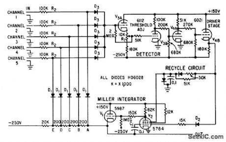
Automatically detects single signal coming from large number of separate sources and identifies source, as required in doppler radar sets that must search bank of sharp filters placed side by side, to detect target, while antenna scans field of search. Positive signal reaching detector is amplified to drive Miller integrator V1-V2. As V1 goes negative, it disconnects one channel at a time (by driving its disconnecting diode D1 below 0 V) until live channel is reached. Detector output is then cut off, and C1 stores level at which disconnect occurred.-R. Kronlage, Monitoring Multiple Inputs Simultaneously, Electronics, 32:35, p 50-51. (View)
View full Circuit Diagram | Comments | Reading(671)
DATA_ENTRY_KEYPAD_ENCODER
Published:2009/7/11 3:59:00 Author:May
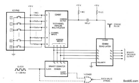
Designed for use in point-of-sale and other data-entry applications requiring bounceless binary encoder.Keypad is scanned by CD4067 16-channel analog multiplexer. When key is depressed, appropriate channel is driven low. When counter ad-dresses low input of multiplexer, common output goes low for one clock cycle. Differentiating network changes this to negative spike for strobing counter data into quad latch where it remains until another key is depressed clockshould be above 200 Hz.-M. E.κeppel, Multiplexer Scans Keyboard for Reliable Binary Encoding, Electronics, March 17,1977,p 99. (View)
View full Circuit Diagram | Comments | Reading(2936)
RECEIVER_INCREMENTAL_TUNING_CIRCUIT
Published:2009/7/17 2:56:00 Author:Jessie
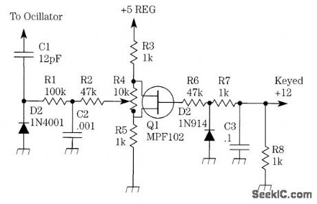


D1 acts as a varactor diode coupled to the transceiver or receiver LO tuning circuit. On receive, Q1, the MPF102, is cut off and the varactor voltage is controlled by the 10-kΩ pot. On transmit, Q1 conducts; this effectively shorts the 10-kΩ pot, placing a fixed voltage on the varactor diode. (View)
View full Circuit Diagram | Comments | Reading(998)
Logarithmic_amplifier_using_an_MC1556_op_amp
Published:2009/7/17 2:55:00 Author:Jessie
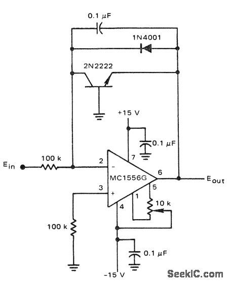
Logarithmic amplifier using anMC1556 op amp. The 10K pot is an offset adjustment (courtesy Motorola Semiconductor Products Inc.). (View)
View full Circuit Diagram | Comments | Reading(832)
SIMPLE_555_VCO
Published:2009/7/11 3:59:00 Author:May
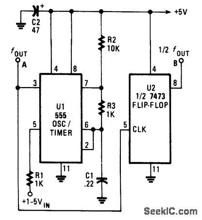
The VCO has an output frequency that ranges from 1 500 Hz at Vin=1 V to 300 Hz at Vin=5V. R1 or C1 can be varied to change this range. U2 provides a symmetrical square-wave output of half the timer frequency. (View)
View full Circuit Diagram | Comments | Reading(1399)
CAPACITANCE_METER
Published:2009/7/17 2:55:00 Author:Jessie
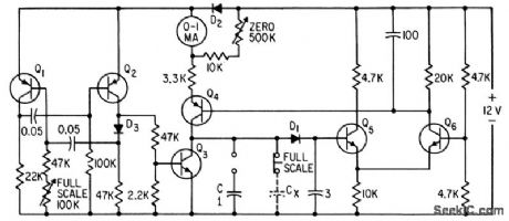
Milliammeter indicates capacitance values over any desired range on linear scale having zero at right.-W. Mosinski, Capacitance Meter has Linear Scale, Electronics, 35:12, p 64. (View)
View full Circuit Diagram | Comments | Reading(4413)
KEYER_WITH_MEMORY
Published:2009/7/11 3:58:00 Author:May
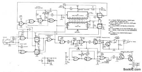
Low-drain CMOS circuit permits storage in RAM of message being keyed, for repeated later use by pushing button.Includes monitor, simple weight control, and both positive and negative keying outputs. Playback of stored message can be interrupted by closing either paddle contact. 1024-bit memory will hold two runs of alphabet, two sets of numbers, and several punctuation marks. Dot is stored as 1 followed.by 0; dash is three is followed by 0, Free-running clock ensures that spaces will be recorded.-C. B. Opal, The Micro-TO MeGsage Keyer, QST, Feb. 1978, p 11-14. (View)
View full Circuit Diagram | Comments | Reading(1102)
FET_TESTER
Published:2009/7/11 3:57:00 Author:May
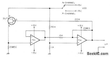
Can be used for measuring JFET pinchoff voltage, matching FETs of same ge-neric type, and measuring bias range of FET. Opamps sense source current of FET under test. First 741 is buffer, while second is preset to 1 V and its output used to drive device under test (DUT) until source current is 100 μA. Polarity of VP is opposite that of VDD.-Circuits, 73Mag-azine, June 1977, p 49. (View)
View full Circuit Diagram | Comments | Reading(7237)
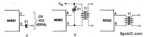
NE602_INPUT_CIRCUITS
Published:2009/7/17 2:50:00 Author:Jessie
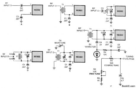
A few of the many ways to input a signal into the NE602. Simple untuned methods (a and b) are acceptable. If you need to tune to a specific frequency, you can use an LC resonant circuit with un-grounded trimmer capacitors (c and d) or with grounded variable capacitors (e). You can even use a tuning voltage in connection with a varactor (f). (View)
View full Circuit Diagram | Comments | Reading(0)
Voltage_controlled_amplifier
Published:2009/7/17 2:50:00 Author:Jessie

This circuit uses one section of an XR-13600 dual OTA as a voltage controlled amplifier. Figure 11-1B shows that both sections of the XR-13600 have predistortion diodes and noncommitted Darlington buffer outputs. In the circuit of Fig. 11-1A, the bias current IB(pins 1 and 16) controls gain of the output. The 1-kΩ potentiometer at the amplifier input is adjusted to minimize the effects (offset) of the gain-control signal at the output. ExAP corporaton Databook, 1990, p 524S 5-252 (View)
View full Circuit Diagram | Comments | Reading(0)
__RESTRICTED_RANGE_VCO
Published:2009/7/11 3:57:00 Author:May

This VCO is adjustable from 60 Hz to 1.4 kHz. C1 can be changed for other ranges (View)
View full Circuit Diagram | Comments | Reading(1300)
Latching_DPDT_switch
Published:2009/7/17 2:48:00 Author:Jessie
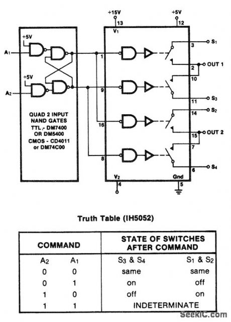
Latching DPDT switch.The A1 and A2 inputs are normally low A high input to A2 turns S1 and S2 on,A highto A1 turns S3 and S4 on,This feature is desirable with limit detectors,peak detectors or mechanical closures(courtesy Intersil,Inc.). (View)
View full Circuit Diagram | Comments | Reading(1046)
NE602_OUTPUT_CONFIGURATIONS
Published:2009/7/17 2:48:00 Author:Jessie
Here are (a) a simplest single-ended approach without impedance matching, (b) a single-ended approach for a tuned LC circuit load, and (c) a balanced approach for better suppression of input and LO signals. (View)
View full Circuit Diagram | Comments | Reading(751)
| Pages:774/2234 At 20761762763764765766767768769770771772773774775776777778779780Under 20 |
Circuit Categories
power supply circuit
Amplifier Circuit
Basic Circuit
LED and Light Circuit
Sensor Circuit
Signal Processing
Electrical Equipment Circuit
Control Circuit
Remote Control Circuit
A/D-D/A Converter Circuit
Audio Circuit
Measuring and Test Circuit
Communication Circuit
Computer-Related Circuit
555 Circuit
Automotive Circuit
Repairing Circuit