
Circuit Diagram
Index 777
POWER_SUPPLY_TESTER
Published:2009/7/11 3:45:00 Author:May
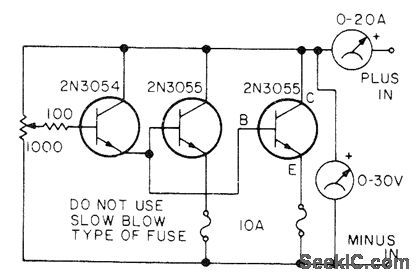
Serves as high-current solid-state-resistor load for testing power supplies before use, to determine voltage and current under load. Darlington configuration of transistors reduces power-dissipating requirements of pot. Use large heatsink for 2N3055s because they must dissipate almost 200 W when powersupply is delivering 15A at 15V.-E. Fruitman, The Smoke Tester, 73 Magazine, Nov, 1976, p 159. (View)
View full Circuit Diagram | Comments | Reading(3347)
INDUCTANCE_METER
Published:2009/7/11 3:43:00 Author:May
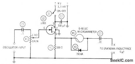
When used with variable-frequency audio oscillator, FET circuit checks any inductance between 60 μH and 60,000 H by resonance method. With unknown coil connected to terminals XX, external oscillator is tuned for peak deflection of M1. Inductance is then calculated from L=1/(395x10-9 f2) where L is in henrys and f is in hertz. if desired, calibration graph can be prepared to eliminate calculations. High input impedance of FET minimizes oscillatorloading. Ad just R1 forfull-scale deflection of meter at resonance, to give maximum sensitivity.-R. P. Turner, FET Circuits, Howard W. Sams, Indianapolis, IN, 1977, 2nd Ed., p 138-140. (View)
View full Circuit Diagram | Comments | Reading(1646)
High_impedance_bridge_amplifier_using_three_MC1556_op_amps
Published:2009/7/17 2:41:00 Author:Jessie
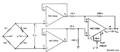
High-impedance bridge amplifier using three MC1556 op amps (courtesy Motorola Semiconductor Products Inc.). (View)
View full Circuit Diagram | Comments | Reading(705)
PULSE_ANALYZER
Published:2009/7/11 3:43:00 Author:May
Either positive or negative pulses equal to or greater than adjustable threshold voltage operate relay ,thus measuring pulse height of either poktrity. Responds to pulse widths as narrow as 50 nsec.Q1 responds to positive pulses, and Q2 to negoiive pulses.-O.B.laug,Pulse Voltage Comparator Measures Height of Positive or Negative Pulses, Electronics, 34:36, p70-71. (View)
View full Circuit Diagram | Comments | Reading(880)
HF_TRANSCEIVER_MIXER
Published:2009/7/17 2:41:00 Author:Jessie
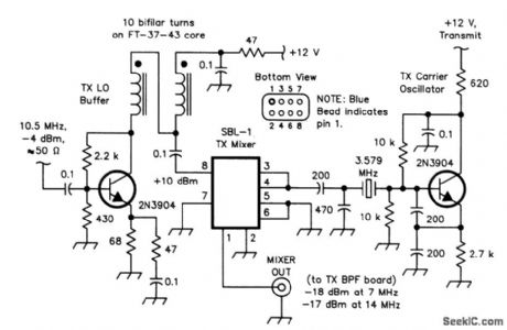
The transceiver mixer and carrier oscillator in the band-imaging (7- and 14-MHz) CW transceiver. Careful selection of drive levels, and use of a spectrally clean carrier oscillator, assure low spurious-signal content in the transmitter output. This transceiver mixer should prove useful in HF and VHF CW or SSB applications. A Mii-Circuits SBL1 low-cost mixer is used with a 3.579-MHz crystal oscillator that uses a low-cost TV color-burst crystal. By paying careful attention to drive leads, good performance and low spurious content can be obtained. (View)
View full Circuit Diagram | Comments | Reading(3794)
SCANNER_VOICE_SQUELCH
Published:2009/7/11 3:42:00 Author:May

This circuit detects the presence of audio (voice) on the output of a scanner. If the scanner stops on a dead carrier or noise, the circuit mutes the speaker to avoid annoying noise.U1 amplifies speech and drives rectifier D1/D2 and switch Q1. Comparator U3 drives speaker switch Q1 and indicator LED1. Q2 completes the speaker path to ground. U2 is an audio amplifier to drive the speaker. R3 is a volume control. PL1 connects to the scanner speaker or to the headphone jack. (View)
View full Circuit Diagram | Comments | Reading(1237)
SIMPLE_VOX
Published:2009/7/11 3:39:00 Author:May
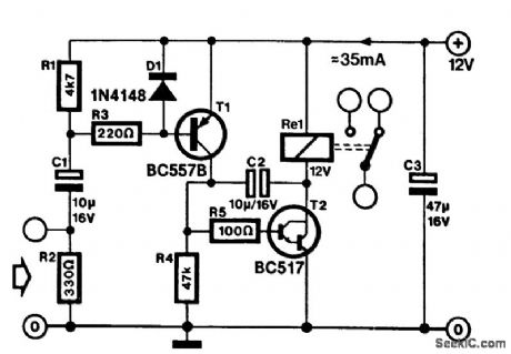
A VOX is a voice-operated switch that is often used as a substitute for the press-to-talk switch on a microphone. This VOX can be connected to almost any audio equipment that has a socket for an external loudspeaker. The actuation threshold is set by the volume control on the AF amplifier that drives the VOX.The (loudspeaker) signal across R2 is capacitively fed to the base of T1. Resistor R3 limits the base current of this transistor when the input voltage exceeds 600 mV. Diode D1 blocks the positive excursions of the input signal, so that Veb cannot become more negative than about 0.6 V.The output relay is driven by Darlington T2. Resistor R4 keeps the relay disabled when T1 is off. The value of bipolar capacitor C2 allows it to serve as a ripple filter in conjunction with T2. Resistor R5 limits the base current of T2 to a safe level.The switching threshold of the VOX is about 600 mV across R2. The maximum input voltage is deter-mined by the maximum permissible dissipation of R2 and R3. As a general rule, the input voltage should not exceed 40 Vpp. The current drawn by the VOX is mainly the sum of the currents through the relay coil and through R5. The resistor can carry up to 100 mA when the VOX is overdriven. (View)
View full Circuit Diagram | Comments | Reading(3117)
Diode_bridge_clamping_circuit_to_improve_A_D_convener_performance_
Published:2009/7/17 2:41:00 Author:Jessie
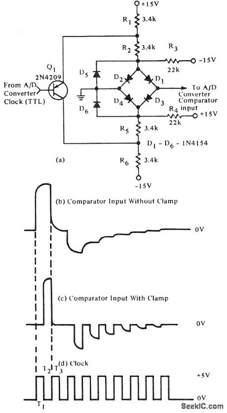
Diode-bridge clamping circuit to improve A/D convener performance (courtesy Burr-Brown Corporation). (View)
View full Circuit Diagram | Comments | Reading(799)
VLF_HF_LIGHTNING_DETECTOR_RECEIVER
Published:2009/7/17 2:40:00 Author:Jessie
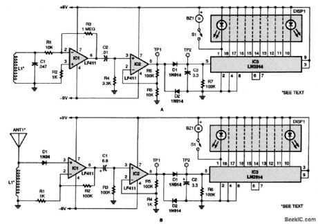
It is known that cloud-to-ground lightning strikes produce far more VLF emissions than cloud-to-cloud strikes. By monitoring both VLF and HE, lightning can be analyzed for such things as strikes per flash, leader steps, amplitude or relative range, and the ratio of cloud-to-ground to cloud-to-cloud discharge. This pair of simple receivers separately monitor both VLF and HE. Note that they are both extremely similar, except for their respective antenna coils. The VLF-antenna coil, L1 in Fig. A, is made of 94 turns of #33 magnet wire wound on an 11-inch-diameter cardboard disk. The HE-antenna coil, L1 in Fig. B, is a common RF choke, or about 100 turns of very fine magnet wire on a X-inch-long ferrite core (any similar junkbox choke should do). Antenna ANTI is a 6-inch wire an-tenna. The first LF411 FET op amps (IC1 in both circuits) are preamps. The second LF411s (IC2 in both) add more gain. Test point 1 in either circuit can be used to connect high-impedance head-phones or an oscilloscope. Test point 2 in either circuit is for a connection to chart recorders or event counters. The outputs of both circuits go to LM3914 bar-graph display drivers (IC3 in both circuits), which power both LED bar graphs (DISP1 in both) and low-voltage piezo buzzers (BZ1, again in both receivers). The negative leads of the buzzers, while shown connected to pin 1, can be connected to any of the bar-graph outputs. Both circuits are powered by split supplies. (View)
View full Circuit Diagram | Comments | Reading(10219)
CHRONOTRON_CIRCUIT_MEASURES_COAX_DELAY
Published:2009/7/17 2:40:00 Author:Jessie
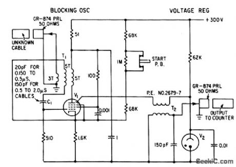
econdary-emission tube V1 (EPP-60) in blocking oscillator generates millimicrosec pulses that are fed to unknown cable through anode transformer. Pulse reflected back from open-circuited end of cable is coupled into grid through same transformer to initiate new pulse. Resulting pulse repetition rate, proportional to cable delay, is measured with 10.Mc digital counter-E. F. Laine, Getting Subnanosecond Precision in Coax Cable Delay Measurements, Electronics, 36:5, p 39-41. (View)
View full Circuit Diagram | Comments | Reading(853)
CHARACTER_READER
Published:2009/7/11 3:35:00 Author:May
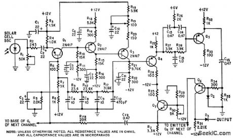


Circuit shows one channel of solar-cell sigmctl amplifier and section of switching bolck for experimental character recognition system.-P.H. Howard, Feedback System Detects 1% Amplitude Difference,Electronics,38:10,p68-70 (View)
View full Circuit Diagram | Comments | Reading(742)
COMPARATOR_FOR_SOLID_SlAlE_DIGITAL_VOLTMETER
Published:2009/7/11 3:31:00 Author:May
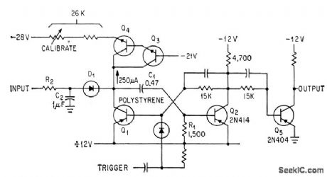
Circuit determines when output of ramp genercttor crosses 0V and crosses unknown voltage. Transistor Q5 isolates mono Q1-Q2 from output iogic. Iransistors Q3 amd Q4 provide constant current for charging C1 linearly to produce high-accurctcy ramp.-R.C. Weinberg, Modified Ramp Generator Develops High D-C input impedance, Electronics, 37:8, p33-35. (View)
View full Circuit Diagram | Comments | Reading(818)
NE6O2_OUTPUT_CIRCUITS
Published:2009/7/17 2:40:00 Author:Jessie
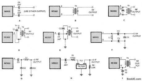
The various output circuits shown here demonstrate how to either pass all the frequencies from the NE602 or allow only the sum or difference frequencies through, depending on which circuit is used.
(View)
View full Circuit Diagram | Comments | Reading(789)
VARIOMETER_RADIO
Published:2009/7/17 2:39:00 Author:Jessie
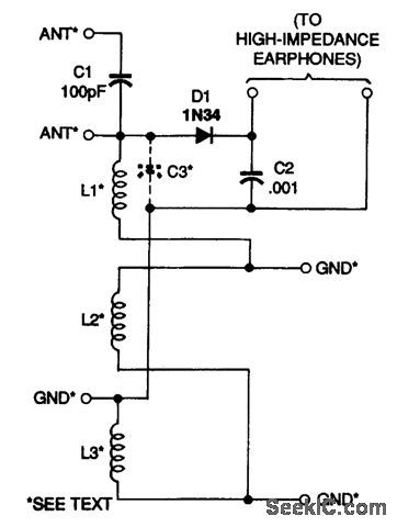
The schematic of the complete variometer radio is shown in the figure. An antenna can be connected to the radio through either of the two points labeled ANT: either directly to the circuit or through a 100-pF capacitor. The ground connection can be made at any of the points marked GND.There is a reason for the preceding options: By varying the antenna capacitance, the ground connection, and the position of the sliding coil, the entire AM broadcast band can be tuned. Depending on the antenna and ground connections, it might be necessary to add a small capacitor, C3, at the point indicated in the schematic. If so, experiment with values between 25 and 200 pF (separately or in parallel) to find which gives the best result. If you build the variometer using Fahnestock clips (as explained later), adding the capacitor(s) after the radio is built if the need arises should be easy. When a signal is selected by adjusting the antenna, ground connection, and position of L2, the signal is passed on to the diode-detector part of the circuit, composed of D1, which demodulates the signal. The signal then goes through bypass capacitor C2 to the earphones. Only high-impedance earphones should be used with the variometer. L1 and L3 are 86 turns of #22 wire on a 1.25-inch form, and L2 is 74 turns of #22 wire on a 1.75-inch form. (View)
View full Circuit Diagram | Comments | Reading(1133)
128_BIT_CODE_STORE
Published:2009/7/11 3:30:00 Author:May
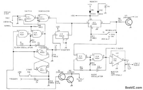
Draws almost no power, can be used on RTTY as well as CW, and can be reprogrammed in less than 1 min. Built around Motorola MC14562CP 128-bit shift register. Combination of 1 (high level) and 0 (low level) bits forming identifier message is fed into of shift register and leave only 0s. Now, set S1 to desired first 1 or 0, push switch PB2 once, and repeat for rest of coded identifier. Set S1 to RECIRCULATE push PB1 to cycle back to starting point, and unit is ready for use. If debouncer is not effective, move its wire from IC1-11 to IC4-10. Easier-to-get altemate values for C1 and R2 are 0.05 μF and 1 megohm.-C. W. Andreasen, Programmable CW ID Unit, 73 Magazine, Oct.1976, p 52-53. (View)
View full Circuit Diagram | Comments | Reading(931)
612AND_30_V_FOR_FM_TUNER
Published:2009/7/17 2:39:00 Author:Jessie
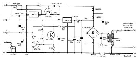
Provides regulated 30 V for voltage-controlled varicap tuning diodes, 12 V for other circuits of tuner, and optional 6 V for stereo decoder. Uses SGS IC regulators. - L. Nelson-Jones, F.M. Tuner Design-Two Years Later, Wireless World, June 1973, p 271-275. (View)
View full Circuit Diagram | Comments | Reading(919)
NE602_DC_BIAS_CIRCUIT
Published:2009/7/17 2:38:00 Author:Jessie

There are several ways to power the NE602. A resistor should be placed in series between the power supply and the NE602 (a and b).A zener diode (c) or a voltage regulator (d) can also be used. The resistor R1 should provide 4.5 to 8.0 V at pin 8 of the NE602. The current draw is about 2.4 to 2.8 mA. (View)
View full Circuit Diagram | Comments | Reading(940)
SIMPLE_MOBILE_RADIO_PROTECTOR
Published:2009/7/17 2:38:00 Author:Jessie
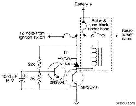
This circuit supplies power to a mobile radio only when the ignition is on and has a delay feature to prevent energizing the radio until the key has been on for several seconds, to avoid spikes and possible transients from the starter motor. (View)
View full Circuit Diagram | Comments | Reading(961)
CW_FILTER_1
Published:2009/7/11 3:28:00 Author:May
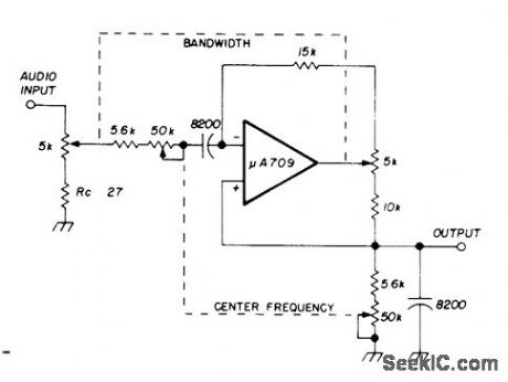
Variable-bandwidth variable-frequency audio filter can be tuned to center frequency anywhere in range from 300 to 3000 Hz.Bandwidth can be as narrow as 50 Hz, which is about 3 times theoretical minimum of is Hz for 50-bit words and Morse code at 25 WPM. Performance can be improved over entire fre-quency range by using 741 opamp.-R. Skelton, Comments, Ham Radio, June 1975, p 56-57. (View)
View full Circuit Diagram | Comments | Reading(925)
3_260_MC_TUNNEL_DIODE_DIP_METER
Published:2009/7/17 2:38:00 Author:Jessie
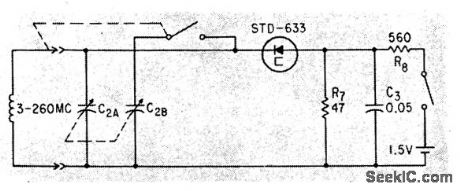
Oscillator is tunable in six ranges, using plug-in circuits.-E, Gottlieb and J. Giorgis, Tunnel Diodes-Using Them as Sinusoidal Generators, Electronics, 36:2A, p 36-42. (View)
View full Circuit Diagram | Comments | Reading(797)
| Pages:777/2234 At 20761762763764765766767768769770771772773774775776777778779780Under 20 |
Circuit Categories
power supply circuit
Amplifier Circuit
Basic Circuit
LED and Light Circuit
Sensor Circuit
Signal Processing
Electrical Equipment Circuit
Control Circuit
Remote Control Circuit
A/D-D/A Converter Circuit
Audio Circuit
Measuring and Test Circuit
Communication Circuit
Computer-Related Circuit
555 Circuit
Automotive Circuit
Repairing Circuit