
Circuit Diagram
Index 775
Stereo_volume_control
Published:2009/7/17 2:48:00 Author:Jessie
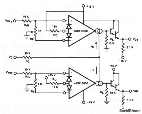
This circuit uses both sections of an XR-13600 (Fig. 11-1B) as a stereo volume control with typical channel-to-channel gain tracking of 0.3 dB. The RP potentiometers are provided to minimize the output offset voltage and they can be replaced with two 510-Ω resistors in ac-coupled applications. With the values shown, amplifier gain is: VO/VIN = 940× IB (mA). EXAR corporation Databook 1990 p 5-253 (View)
View full Circuit Diagram | Comments | Reading(1153)
30_MHz_IF_PREAMP
Published:2009/7/17 2:47:00 Author:Jessie
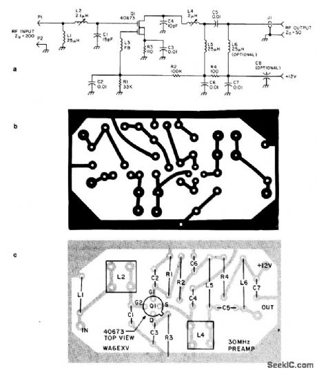
This preamp for 30 MHz is useful for IF applications used in microwave work, etc. A 40673 MOSFET is used and typically the gain at 30 MHz will be 20 to 25 dB. (View)
View full Circuit Diagram | Comments | Reading(874)
SAWTOOTH_CLIPPER
Published:2009/7/17 2:47:00 Author:Jessie
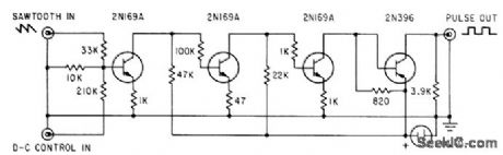
High-gain amplifier converts sawtooth input to rectangular out.put pulse whose width is proportional to portion of sawtooth amplitude that is above threshold level.-B. E. Mathews and F. R. Sias, Jr., Testing Space Craft with Induction Heaters, Electronics, 35:34, p 38-41. (View)
View full Circuit Diagram | Comments | Reading(760)
TUNED_OUTPUT_NE602_CIRCUITS
Published:2009/7/17 2:47:00 Author:Jessie
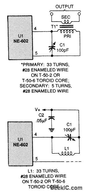
A tuned output like this one will reject all but the desired output signal.
Here is a single-ended tuned-output circuit. (View)
View full Circuit Diagram | Comments | Reading(747)
TRANSISTOR_AND_DIODE_TESTER
Published:2009/7/11 3:56:00 Author:May
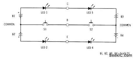
Four pairs of,AA penlight cells provide power for testing transistors and diodes quickly for opens and shorts. Circuit also distinguishes between PNP and NPN transistors and shows diode polarity. Leads of diode are inserted into base and collectoriacks (B and C), and switches are prqssed in succession. If LED 1 glows, diode is good and its anode lead is in collector jack. If LED 3 glows when S2 is pressed, anode of diode is in base jack. If both LEDs glow, diode is shorted. If neither LED glows, diode is open. With transistor in tester, unit is PNP if LED 1 and LED 2 glow. If LED 3 and LED 4 glow, unit is NPN. If one or no LEDs glow, transistor is open. If three or more LEDs glow, transistor has shorted junction. Any LEDs can be used.-F.M. Mims, Transistor Projects, Vol. 3, Radio Shack, Fort Worth, TX, 1975, p 87-93. (View)
View full Circuit Diagram | Comments | Reading(945)
IF_AMPLIFIERIER
Published:2009/7/17 2:47:00 Author:Jessie
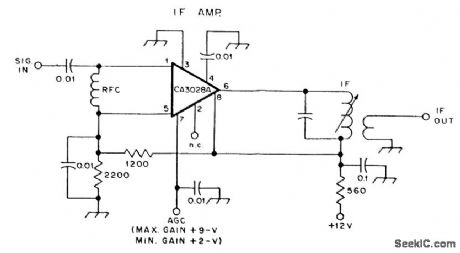
Using a CA3028A,this circuit is useful up to about 15 or 20 MHz. (View)
View full Circuit Diagram | Comments | Reading(1279)
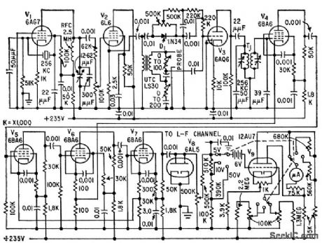
REGENERATIVE_SHORTWAVE_RECEIVER
Published:2009/7/17 2:46:00 Author:Jessie
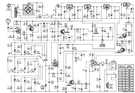
The receiver is composed of several subassemblies: an active antenna, an amplifier (with a regeneration control and band-switching circuitry), an AM detector, a power amplifier, and some form of output device (internal speaker, external speaker, or phones), plus a multivoltage power supply. The schematic diagram of the receiver is shown in the figure, a dual-gate MOSFET, Q4 (which is analogous to a pentode vacuum tube), is used as the regenerative amplifier. The dual-gate MOSFET is configured as a Colpitts oscillator, rather than an Armstrong type. The MOSFET's feedback from source to gate is provided via R18 and C33. The circuit contains several standard fixed-value inductors, each of which is connected in parallel with a small variable capacitor. Those LO pairs along with a SP12T rotary switch (S2) are used for band selection. Regenerative amplification and AM detection are performed by two separate transistors, Q4 and Q5. The AM detector (which is called an infinite-irnpedance detector) has the advantage of not loading the RF stage appreciably, Because D3 is operated with a slight forward bias, either a germanium or a silicon diode can be used in that position. The dc voltage across R24 (the volume control) should be about 0.1 V. Regeneration is controlled by varying the voltage applied to gate 2 of Q4. The circuit also contains fine and coarse regeneration controls that allow delicate adjustments. The receiver uses an active-antenna circuit, consisting of transistors Q1, Q2, and Q3. Under most conditions, a short whip antenna is adequate. (View)
View full Circuit Diagram | Comments | Reading(5179)
RECEIVER_IF_AMPLIFIER
Published:2009/7/17 2:46:00 Author:Jessie
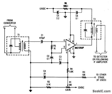
T1 is tuned to converter-output frequency U1 to provide 45-to-50-dB gain, depending on the design of T1 and T2. C2, C3, C4, CS, and C6 are bypass capacitors. R5 is a bias resistor. Gain is set by R1, which controls the voltage on pin 5 of U1. T1 and T2 should provide source and load impedance of 1-kΩ and 3-to 10 kΩ, respectively. R3 supplies dc bias to other stages, if required. (View)
View full Circuit Diagram | Comments | Reading(880)
CABLE_TERMINATION_FOR_VELOCIMETER
Published:2009/7/17 2:46:00 Author:Jessie
Amplifier restores leading edge of sinusoidal signal that has travailed through up to 35,000 feet of cable from deep-sea velocimeter. Frequency is then doubled by diodes, for ease of counting.-L. Dulberger, DeepOcean Velocimeter Aids Sonar Systems Design, Electronics, 34:22, p 41-43. (View)
View full Circuit Diagram | Comments | Reading(720)
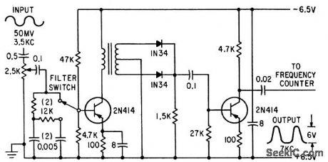
1_kHz_TONE_DECODER
Published:2009/7/11 3:56:00 Author:May
Used as interface between amateur CW receivel and Motolola 6800 microcomputer to copy any code speed from 3 to 60 WPM while adjusting automatically to irregularities of hand-sent code. Translation program given in article requires about 600 bytes of memory. Algorithm can be converted to run on almost any 8-bit microprocessor. Tone decoder is 567 phase-locked loop tuned to center frequency of about 1 kHz, with bandwidth of about 100 Hz. Circuitwill switch fast enough for most code speeds. PLL gives noise immunity.Optimum input level is about 200 mV. Output rests at +5 V dropping near ground when tone of correct frequency is detected.-R, D. Grappel and J. Hemenway, Add This 6800 MORSER to Your Amateur Radio Station, BYTE, Oct. 1976, p 30-35. (View)
View full Circuit Diagram | Comments | Reading(2312)
CODE_REGENERATOR
Published:2009/7/11 3:55:00 Author:May

Converts noisy CW output of receiver into TTL 1 s and 0s for driving automatic Morse-code printer. Clipper U1A and 800-Hz active bandpass filter U1B feed injection-locked 800-Hz phase-shift oscillator U3 (National LM7401CN or Motorola HEP-C6052P).U1 is LM1458N or MC1458P. U2 uses part of LM709CN or HEP-C6103P as matched pair of 7-V back-to-back zener diodes. Diode detector D1 has time constant of about 5 ms, which is short enough for highest Morse-code speeds. Detector feeds LM311N or MLM311P1 voltage comparator U4 which can drive TTL or DTL directly, National LM380N audio amplifier U5 allows CW signal to drive loudspeaker directly.-H. Olson, CW Regen erator/Processor, 73 Magazine, July 1976, p 80-82. (View)
View full Circuit Diagram | Comments | Reading(1164)
UJT_PULSE_SHAPER
Published:2009/7/17 2:54:00 Author:Jessie
Use of inductance in ujt relaxation oscillator gives significant improvement in output pulse shape over that of conventional resistance-coupled circuit. Pulse width for various transistors is between 11 and 12 microsec, and rise and fall times are typically 0.3 microsec. With 47-ohm resistor in place of inductance, fall time would be 3 microsec.- Transistor Manual, Seventh Edition, General Electric Co., 1964, p 316. (View)
View full Circuit Diagram | Comments | Reading(2275)
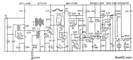
PORTABLE_FLOWMETER
Published:2009/7/17 2:54:00 Author:Jessie

Impedance between gold wire and blades of water-driven propeller changes a small amount as each blade passes within 0.1 mm of wire tip, giving amplitude modulation of 15-kc car rier generated by Q1. After demodulation,signal at propeller frequency is amplified, rectified, and integrated to drive velocity-indicating meter.-L. Molyneux and J. M.Edington, Portable Propeller Flowmeter Determines Water Velocity, Electronics, 34:25, p 60-62. (View)
View full Circuit Diagram | Comments | Reading(858)
TUNED_INPUT_CIRCUITS_FOR_NE6O2
Published:2009/7/17 2:54:00 Author:Jessie
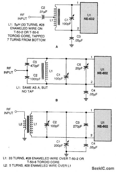
Here are three tuned input circuits. A tapped-inductor LC tuned circuit is shown in A and a flexible-tuned input circuit that can be used in a variety of situations is shown in C. (View)
View full Circuit Diagram | Comments | Reading(782)
PULSE_LENGTH_CONTROLLER
Published:2009/7/17 2:53:00 Author:Jessie
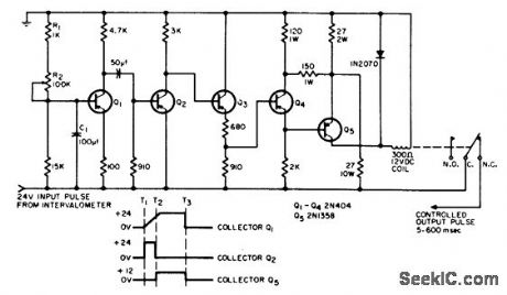
Reduces duration of intervalometer pulse from 400 millisec to 100 millisec without affecting intervalometer operation for other purposes Used to control airborne strip-chart camera.-J. S. Peddo, Low-Cost Pulse-Length Controller, EEE, 12:7, p 26. (View)
View full Circuit Diagram | Comments | Reading(864)
NE6O2_RF_INPUT_CONFIGURATIONS
Published:2009/7/17 2:53:00 Author:Jessie
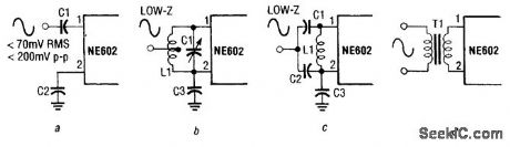
Here, (a) to (c) are for single-ended coupling, with (a) being for no impedance matching, (b) for tnductive matching, and (c) for capacitive matching. By contrast, (d) is a balanced input with reduced second harmonic. (View)
View full Circuit Diagram | Comments | Reading(650)
Logarithmic_amplifier_using_an_MC1S39G_op_amp_
Published:2009/7/17 2:52:00 Author:Jessie
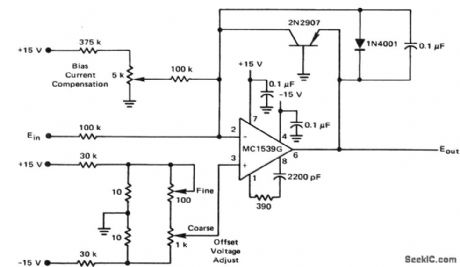
Logarithmic amplifier using an MC1S39G op amp (courtesy Motorola Semiconductor Products Inc.). (View)
View full Circuit Diagram | Comments | Reading(680)
THICKNESS_GAGE_COMPENSATOR
Published:2009/7/17 2:52:00 Author:Jessie
High-frequency channel (256 kc) compensates for variation in probe-to-specimen spacing in eddy-current thickness gage for measuring cladding on reactor fuel elements.-W. J.McGonnagle, C. J. Renken, and R. G. Myers, Improved Nondestructive Testing by Eddy-Currents, Electronics, 32:35, p 42-43.
(View)
View full Circuit Diagram | Comments | Reading(762)
Amplitude_modulator
Published:2009/7/17 2:52:00 Author:Jessie
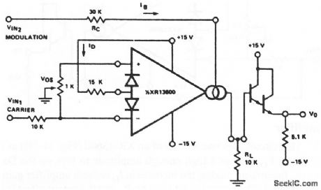
This circuit uses one section of an XR-13600(Fig.11-1B)and an amplitude modulator (or two-quadrant multiplier), where IO=(-2IS/ID) ×(IB) EXAR Corporation Databook, 1990 p 5-253 (View)
View full Circuit Diagram | Comments | Reading(0)
BROADBAND_NE602_SINGLE_ENDED_OUTPUT_CIRCUITS
Published:2009/7/17 2:51:00 Author:Jessie
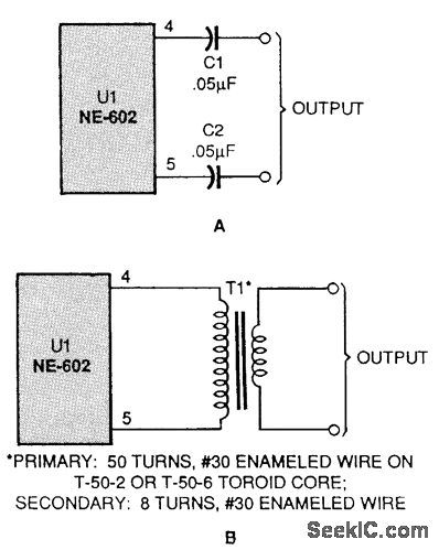
Here are two single-ended output circuits. A capacitor output is shown in A and a single-ended transformer output is shown in B. (View)
View full Circuit Diagram | Comments | Reading(706)
| Pages:775/2234 At 20761762763764765766767768769770771772773774775776777778779780Under 20 |
Circuit Categories
power supply circuit
Amplifier Circuit
Basic Circuit
LED and Light Circuit
Sensor Circuit
Signal Processing
Electrical Equipment Circuit
Control Circuit
Remote Control Circuit
A/D-D/A Converter Circuit
Audio Circuit
Measuring and Test Circuit
Communication Circuit
Computer-Related Circuit
555 Circuit
Automotive Circuit
Repairing Circuit