
Battery Charger
Index 5
Pulse express charger circuit diagram
Published:2011/9/7 7:02:00 Author:Vicky | Keyword: pulse, express charger
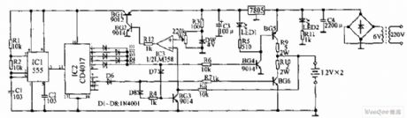
Pulse express charger circuit is shown in the above picture. This nickel-cadmium battery charger can reduce undesirable polarization and prolong the lifetime of battery. In the circuit, 555 are connected and form astable vibrator, which is uses as clock with frequency of about 500Hz. The astable vibrator controls decimal counter CD4017 to output square wave pulse. It then conducts high-current pulse charging and discharging with a proportion of 5:1 to the nickel-cadmium battery after amplified by power tube. There are intermittent pauses during the charging and discharging. During the pauses,check the voltage of the battery by the calculating amplifier. When the battery is full charged, the circuit automatically stops charging. (View)
View full Circuit Diagram | Comments | Reading(3455)
Circuit diagram of 9V charger which can preset the end voltage of charging
Published:2011/9/7 4:00:00 Author:Vicky | Keyword: 9V charger, preset the end voltage of charging

The picture is a circuit of 9V charger which can preset the end voltage of charging. The charger has four groups of identical charging circuit, which can charge four pieces of PP3 type 9V nickel-cadmium battery at the same time. The end voltage can be set between 8.5 to 10V. The voltage comparators IC2A~IC2D constitute four groups of charging circuit with T1~T4 respectively. Every circuit can charge a PP3 type 9V nickel-cadmium battery. 15V DC voltage is divided by voltage divider composed of R17, P1, R18, and D1. The base voltage of 8.5~10V can be gained in the sliding end by adjusting P1. The voltage is added to non-inverting input ends of the four comparators by four 100KΩ isolation resistance. The voltage of every group charged is added to inverting end of its corresponding comparators via a 100KΩ resistance to compare with the base voltage. (View)
View full Circuit Diagram | Comments | Reading(2114)
Express charger circuit diagram
Published:2011/9/7 3:58:00 Author:Vicky | Keyword: Express charger circuit
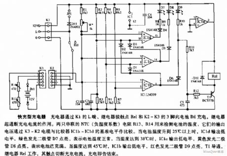
Express charger circuit diagram
The charger charges Bt1via the Lend of K1, contact point Rel of relay, and pin 3 of K2-K3, while the relay acts to control on-off of the charging current. Two NTC (negative temperature coefficient) resistances R13 and R14 in serial are used to examine the temperature of battery. Their output voltage compares with the base level of comparators IC1b ~IC1d via wire cable K3 ~ K2. When the battery temperature rises to above 25℃, IC1d outputs low level, and the green luminous diode D7 is lighted to show that the battery temperature is normal. When the temperature rises to 38℃, IC1c outputs low level, and yellow luminous diode D8 is lighted to show that the battery is full charged. When the temperature rises to 45℃, IC1b outputs low level, the red luminous diode D9 is lighted, T1 is conducted, relay Rel starts working with its contact point cutting off the charging current, and the charging ends. (View)
View full Circuit Diagram | Comments | Reading(1433)
Diagram of lithium battery protection circuit based on Xysemi XB4251A
Published:2011/9/7 8:09:00 Author:Vicky | Keyword: lithium battery, protection circuit
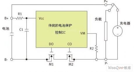
Schematic of lithium battery protection devices is shown in the above picture, which is realized mainly by battery protection control IC , exterior discharging switch M1 and charging switch M2. When P+/P- end is connected with charger, M1 and M2 are all under conducting state when the battery is charged normally; when the control IC detects any abnormality during charging, M2 is then cut off and charging process stops. When P+/P- end is connected with load, M1 and M2 are all under conducting state when the battery is discharging; when the control IC detects any abnormality, M1 is cut off and discharging process stops.
In addition, XB4301 cannot be reversely connected. XB4301 is mainly used in MP3 and Bluetooth at present, including partial mobiles, GPS application. (View)
View full Circuit Diagram | Comments | Reading(2234)
Portable Multi-charging Circuit Made Of LS325A
Published:2011/9/6 6:55:00 Author:Felicity | Keyword: Portable, Multi-charging
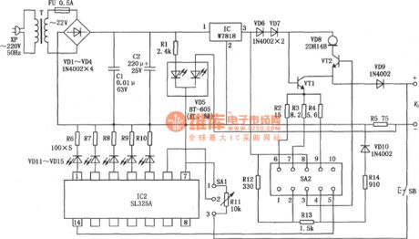
View full Circuit Diagram | Comments | Reading(996)
Sun Battery Charger Circuit
Published:2011/7/23 6:47:00 Author:Michel | Keyword: Sun Battery, Charger Circuit
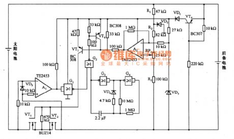
The above picture is sun battery charger circuit.Electronic filter (VT5) and regulating diode,VD3 constitute regulating circuit.Its stable voltage is used as benchmark voltage of A2 reverse phase input terminal.Measuring battery voltage of resistance R1,R2,R3 and RP1 are added to A2 phase input terminal. When it is lower than benchmark voltage,A2 outputs low PWL,VT3,VT1 and VT2 conduct.If the sun battery voltage is higher than the backup battery voltage,it begins to charge the backup voltage.A1 test sun battery voltage is lower thsn backup battery voltage,A1 outputs low PWL.G3 and G4 are harmonic oscillators and it produces 15 ms pulse every 15s.A1 compares backup battery voltage and the sun battery voltage,for example,VT1 and VT2 is still in cut-off condition if sun battery is lower than backup battery. (View)
View full Circuit Diagram | Comments | Reading(1864)
Automatic Ni-Cd Battery Charger Circuit Diagram
Published:2011/8/9 21:28:00 Author:Vicky | Keyword: Automatic Ni-Cd Battery Charger
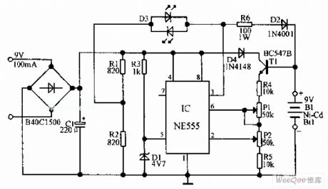
Automatic Ni-Cd Battery Charger circuit is shown in the above picture. The internal comparator of NE555 is set as 4.7V by Zener diode. If the potential of pin 6 becomes higher than this value, the output of pin 3 become lower; if the potential of pin 2 is lower than half of the reference voltage, the output voltage becomes higher,. When the voltage of the under-charging battery is very low, the output potential of the IC is high, the battery is charged via R6 and D2 until it’s full-charged. The voltage is set by P2, the state of output of IC is then changed, and the charging process stops. But IC still control the battery temporarily via T1. When the battery output reduces to the level set by P2 due to self-discharging, IC restart charging. (View)
View full Circuit Diagram | Comments | Reading(6997)
NEC mobile charger circuit diagram
Published:2011/8/4 21:10:00 Author:Sophia | Keyword: NEC mobile charger
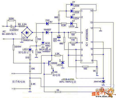
NEC mobile phone charger circuit is shown as below When C1 selected 2.2? F/250V AC step-down capacitor, the output current is about 130mA. Mobile phone battery charging time can be easily selected according to the capacity, so the battery will not be damaged. Specific discharge functions can extend nickel-cadmium battery life with the memory effect. Charging power is indicated by the four high-brightness light-emitting diode level indication, which is very intuitive. In the charging circuit, the AC depressurization capacitor and discharge control tube C8550 are delicate components. When we need to maintain these two components, we can use comprehensive similar component to replace them. (View)
View full Circuit Diagram | Comments | Reading(3873)
Nokia 8210 mobile phone travel charger circuit diagram
Published:2011/8/4 21:20:00 Author:Rebekka | Keyword: travel charger, Nokia mobile phone
The Nokia 8210 mobile phone travel charger produced by Shanghai has been marked on the shell: input AC220V/50Hz(≤30mA),output 4.2V(≤200mA). When people use it to charge the 3.6V rechargeable lithium battery, the red light will be turned off and green light turned on when the it is charged to 3.98V. the whole charging time is about 4 hours. The op amp in the circuit is used as the comparator.
(View)
View full Circuit Diagram | Comments | Reading(5716)
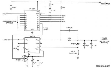
STEP_UP_SUPPLY_BATTERY_CHARGER
Published:2009/7/13 23:16:00 Author:May
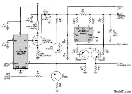
IC1 is a step-up switching regulator that boosts Vin (nominally 5 V) as necessary to supply the combination of charging current and load current. The 5-V source must include short-circuit protection. IC2 is a high-side current-sense amplifier that monitors the charging current. Commands from the processor include. CHARGE ON/OFF and FAST/TRICKLE CHARCGE. IC2 produces an output current (OUT) equal to 10-4 of the current through sense resistor R9. Q3 and Q4 are on during a fast-charge operation, so this output current flows through the parallel combination of R11 and (approximately) R4. The resulting feedback to IC1 (pin 3) maintains the fast-charge current through R9 at 500 mA. This feedback also enables the regulator to supply as much as 500 mA of load current in addition to the fixed 500 mA of charging current. Q2 limits the battery voltage to 10 V (2 V/cell). During the fast charge, an external processor and multichannel A/D converter (ADC) must monitor the battery's terminal voltage. When the ADO senses a change of slope in this voltage, the processor terminates the fast charge by asserting a high on FAST/TRICKLE CHARGE. Q3 turns off, causing a rise in the feedback (FB) that lowers the charging current to the trickle charge rate (approximately 60 mA). If IC1 shuts down or if the load current plus charging current exceeds the capability of IC1, the R9 current reverses as current flows out of the battery. IC2 indicates the reversal by allowing R13 to pull its open-collector SIGN output high, turning off Q4 and turning on Q5. Current through R12 then produces a voltage proportional to the battery's discharge current (5 A through R9 produces a full-scale response of 3 V across R12). By integrating this voltage over time (sampling at fixed intervals and multiplying by the time interval), the A/D-processor system can monitor energy removed from the battery. Based on this measurement and the terminal-voltage measurement, the processor can then reinitiate a fast charge (by asserting FAST/TRICKLE CHARGE low) before the battery reaches its end of life.
(View)
View full Circuit Diagram | Comments | Reading(1551)
PRECISION_Li-ION_BATTERY_CHARGER
Published:2009/7/13 22:14:00 Author:May

An alternative to using expensive 0.25-percent precision resistors is presented in this battery-charger design, which adds two 1-percent resistors and two jumpers to the charger.In constant-voltage-mo de charging, a lithium-ion cell requires 4.1 V ±50 mV. The 1.2-percent requirement represents a tight tolerance. In a regulation loop where a voltage divider is compared against a reference, the accuracy is typically achieved by selecting a 0.7-percent reference and a volt-age divider with 0.25-percent tolerance resistors. Unfortunately, 0.25-percent precision resistors cost three times as much as 1-percent resistors and have very long lead times. One solution for moderate-volume production involves adding two 1-percent resistors and two jumpers to the charger circuit (see the figure). The jumpers are removed as necessary to bring the constant voltage to the required accuracy of 1.2 percent. The charger selected for this example is the LT1510. There are three lithium-ion cells in the. battery. After a value is selected for R4 the values for R1, R2, and R3 can be calculated using the equations given. K is the relative change required for a circuit with all of its tolerances in one direction. For example, in the case of a 0.5-percent reference and two 1-percent resistors, the total tolerance is 2.5 percent. To bring it back to 1.2 percent, the percentage change required is 2.5 percent - 1.2 percent 1.3 percent, and K =0.013. The jumpers (J1 and J2) must be opened based on the following:If VOUT is K/2 below nominal, remove J1.If VOUT is K/2 above nominal, remove J2.The following values were calculated: R1 = 4.99 kΩ, R2 = 324Ω,R 3=80.6 ,Ω and R4= 20 KΩ The voltage below which jumper J1 should be opened is 12.34 V -1.3 percent /2 = 12.22 V. The voltage above which jumper J2 should be opened is 12.34 V + 1.3 percent /2 = 12.42 V. (View)
View full Circuit Diagram | Comments | Reading(1832)
195_V_FROM_27_V_BATTERY
Published:2009/7/13 3:43:00 Author:May
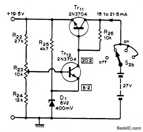
Used to provide precise voltage levels required by portable trigger unit designed to fire up to five different flash units at equal intervals that may range from 11 ms to 11 s. Article gives all circuits.-R. Lewis, Multi-Flash Trigger Unit, Wireless World, Nov.1973, p 529-532.
(View)
View full Circuit Diagram | Comments | Reading(1031)
INPUT_PULSE_UNBALANCES_BRIDGE
Published:2009/7/16 5:45:00 Author:Jessie
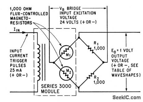
Trigger pulse causes opposite resistance variations in magnetoresistors M1 and M2, to give 1 v output for 25-ma pulse current.-R. M. Gitlin, Magnetoresistors Isolate Load From Control Circuit, Electronics, 38:3, p 60-61. (View)
View full Circuit Diagram | Comments | Reading(1009)
CRYSTAL_PARAMETER_BRIDGE
Published:2009/7/16 5:41:00 Author:Jessie
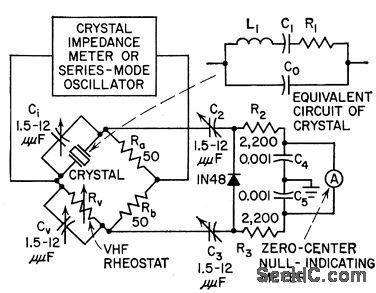
Bridge plugs into crystal socket of standard crystal impedance meter, and crystal under test plugs into bridge. Only other instruments needed for measuring equivalent parameters of overtone crystals for 75 to 200 Mc are frequency meter and null-indicating meter.-D. W. Robertson, Plug-in Bridge Checks VHF Quartz Crystals, Electronics, 31:19, p 82-85. (View)
View full Circuit Diagram | Comments | Reading(1290)
BATTERY_SWlTCH_OFF
Published:2009/7/12 21:39:00 Author:May
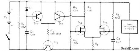
Can be added to any battery-operated device to eliminate unnecessary running down of costly batteries when someone forgets to tum switch off manually. Circuit shown gives operating time of about 10 hours ,permitting use of equipment for full working day without interruption. Normal operation can be restored after shut-off byturning manual switch off and then on again. When circuit has switched off, only battery drain is current through 10-megohm resistor R1 and leakage through transistors. Time of switch-off can be changed by altering C2 or R7. Tr1 and Tr2 are 2N4061, BC478, or similar PNP silicon; Tr3 is 2N3053, BC142, or similar medium-power NPN silicon; Tr4 and Tr5 are 2N3819; D1 is any small silicon diode; R6 is 4.7K for 9-V or 12-V battery, and 10K for 15-V to 27-V battery. R2 is chosen to suit working current and battery voltage; suitable value is 15Vb/Iout.-D, T. Smith, Automatic Battery Switch-Off Circuit, Wireless World, April 1976, p 76.
(View)
View full Circuit Diagram | Comments | Reading(1218)
Signal_level_envelope_detector
Published:2009/7/17 3:21:00 Author:Jessie
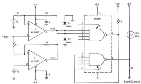
Signal-level envelope detector. The MC1535G is a dual op amp and the MC844P a dual power gate. This circuit indicates by way of the lamp when the input signal is out of range (courtesy Motorola Semiconductor Products Inc.). (View)
View full Circuit Diagram | Comments | Reading(1456)
60_hertz_nicad_battery_charger_with_voltage_sensing
Published:2009/7/17 3:49:00 Author:Jessie
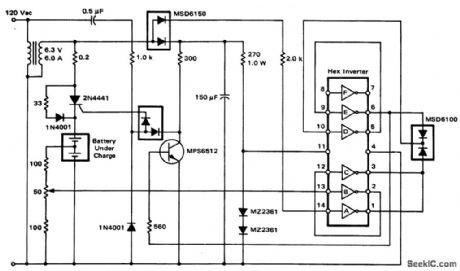
60-hertz nicad battery charger with voltage sensing. Hex inverter is an MC789P (courtesy Motorola Semiconductor Products Inc.). (View)
View full Circuit Diagram | Comments | Reading(1013)
12_volt_battery_charger_with_an_SOB_and_a_PUT_
Published:2009/7/17 3:44:00 Author:Jessie
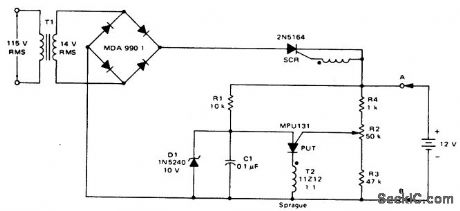
12-volt battery charger with an SOB and a PUT (courtesy Motorola Semiconductor Products Inc.). (View)
View full Circuit Diagram | Comments | Reading(1144)
JONES_CHOPPER_FOR_BATTERY_POWERED_VEHICLE
Published:2009/7/10 22:58:00 Author:May
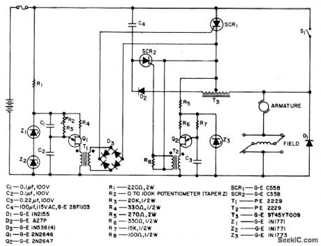
Uses variable-frequency constant pulse-width system that starts reliably and provides smooth acceleration. At low speeds, on time of chopper, in series with d-c series motor,is much less than off time so average motor voltage is low. Potentiometer R2 controls ratio of on to off limes for speed control. Silicon Controlled Rectifier Manual, Third Edition, General Electric CO,1964, p173. (View)
View full Circuit Diagram | Comments | Reading(1699)
±15_V_AND_5_V_CAR_BATTERY_SUPPLY
Published:2009/7/10 20:52:00 Author:May

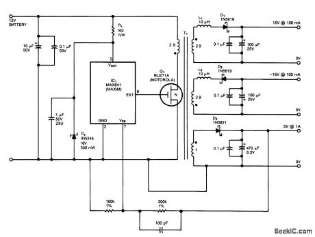
IC1is a switching regulator that generates a 45-kHz signal that drives the gate of MOSFET Q1.D1,D2, and D3 are Schottky diodes. The 5-V output is sensed as a reference; feedback to the chip turns offthe gate signal to Q1 if the voltage nses above 5 V.
T1 has Trifilar windings that assume about 2% regulation fr a 10-to 100-mA load change on the±15-V supplies, R1/D4 provide overvoltage protecti. T1 has a pnmary inductance ofabout 21 μH. Coreslze should allow 4-A peak currents. The turn ratios are 11 1/2 turns each for the 15-V supplies. 11 1/2 turns for the pnmary, and four turns for the 5-V secondary. The efficiency is about 75%. (View)
View full Circuit Diagram | Comments | Reading(1080)
| Pages:5/13 12345678910111213 |
Circuit Categories
power supply circuit
Amplifier Circuit
Basic Circuit
LED and Light Circuit
Sensor Circuit
Signal Processing
Electrical Equipment Circuit
Control Circuit
Remote Control Circuit
A/D-D/A Converter Circuit
Audio Circuit
Measuring and Test Circuit
Communication Circuit
Computer-Related Circuit
555 Circuit
Automotive Circuit
Repairing Circuit