
Index 237
WIEN_BRIDGE_FILTER
Published:2009/7/8 3:24:00 Author:May
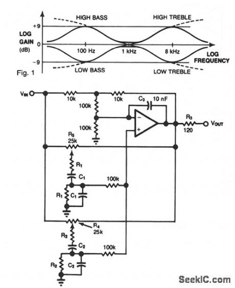

Most audio tone controls affect midband gain, and they often create booming or hissing sounds when activated. You can avoid these problems by using a dual Wien-bridge filter to provide independent control of the treble and bass frequencies.Experiments with equalizers indicate that the optimum center frequencies are about 100 Hz and 8 kHz. Using the relationf = (2πRC)-1, set the Fig. 1 values accordingly:
100 Hz: R1 = 15 KΩ; C1 = 0.1 μF 8 kHz: R2 = 16 KΩ; C2 = 1.3 μFR3 and C3 provide stability. You obtain a ± 9 dB variation of treble and bass by adjusting potentiometers R4 and R5, respectively. The filter's frequency response is shown in Fig. 2. (View)
View full Circuit Diagram | Comments | Reading(1694)
OVERSHOOT_COMPENSATION
Published:2009/7/8 3:24:00 Author:May
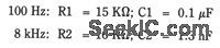
Used to control temperature of industrial gas-fired heater having very high thermal capacity. When AD311 opamp comparator trips at set-point temperature, 555 mono makes transistors turn on gas solenoid and light burner. When mono times out, burner goes off regardless of opamp output condition, Time constant of 555 compensates for lags in system by turning off heater before AD590 sensor reaches cutoff value, Thermistor across 555 mono compensates for changes in ambient temperature. During start-up, AD741 opamp and associated circuit effectively by-passes mono, and also turns on heater if mono fails to fire for any reason.-J. Williams, Designer's Guide to: Temperature Control, EDN Magazine, June 20, 1977, p 87-95.
(View)
View full Circuit Diagram | Comments | Reading(1189)
THERMISTOR_BRIDGE
Published:2009/7/8 3:21:00 Author:May
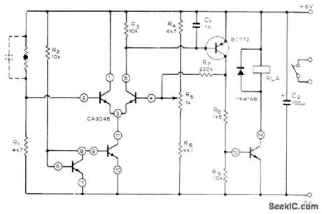
Bridge is formed by thermistor with R1, R4, R5, and R6. Unbalance is sensed by CA3046 IC having two matched pairs of transistors, with additional output transistor in IC. Positive feedback through R7 prevents chatter as switching point is approached. R5 sets switching temperature precisely. Relay comes on when temperature drops below pre determined point; for opposite function, reverse positions of thermistor and R1. Value of R1 is chosen to give approximately the desired control point.-D. E. Waddington, Thermistor Controlled Thermostat, Wireless World, July 1976, p 36.
(View)
View full Circuit Diagram | Comments | Reading(1112)
SSB_MONITOR
Published:2009/7/21 21:24:00 Author:Jessie
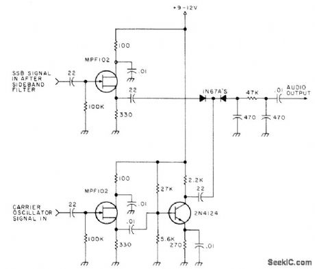
Requires two connections to SSB transmitter, at output of carrier oscillator and at output of sideband filter. FET isolation stages for each connection feed 2N4124 product detector that gives audio signal for monitoring directly with headphones or for feeding AF amplifier driving loudspeaker,-Clean Up Your Act,73 Magazine.Jan 1978,p136-137. (View)
View full Circuit Diagram | Comments | Reading(1056)
TEN_BAND_OCTAVE_EQUALIZER
Published:2009/7/8 3:16:00 Author:May
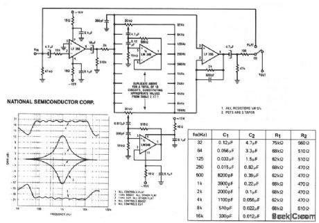
A series of active rf filters using National LM348IC comprises a ten-band graphic equalizer. C1, C2, R1, and R2 should be at least 10% with 5% preferred tolerances. (View)
View full Circuit Diagram | Comments | Reading(1809)
144_175_MHz_80_W_SINGLE_STAGE_FM_MOBlLE
Published:2009/7/8 3:15:00 Author:May
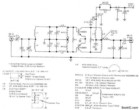
Provides rated outputinto 50-ohm load,Can withstand open and shorted loads for all load phase angles without transistor damage Uses Motorola 2N6084 land,mobile transistors optimized for 12.5-V FM operation. Transistors are used in parallel with single-ended input and output, isolated from each other by signal-split-ting coils.—J. Hatchett, VHF Power Amplifiers Using Paralleled Output Transistors, Motorola, Phoenix, AZ, 1972, AN-585, p 2. (View)
View full Circuit Diagram | Comments | Reading(2279)
THERMAL_CYCLER
Published:2009/7/8 3:12:00 Author:May
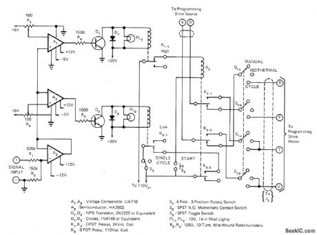
Circuit allows operator to preselect uipper and lower temperature limits for controller used in determining effect of continuous thermal cycling on properties of materials.Switching arrangement gives choice of ranging from manual to fully automatic continuous cycling.Operation of programming drive motor is controlled by continuous of relay K3.When relay is energized, motor runs in forwardd irection to increase temperature;when deenergized, motor is reversed. Condition of K3 tinuous depends on which of limit relays K1 or K2 was most recentiy energized . Control circuit samples output of temperature programmer; this DC input signal is reduced to 5 V maximum by R1-R2 and amplified by voltage follower A3 Signal is then compared in A1 and A2 to continuously variable reference voltage from 0 to 5 V preselected by 10-turn pots R3and R4. Q1 is cut off when input is below reference. When input exceeds reference, Q1 goes on and energizes upper-limit relay K1 Article gives initial setup procedure.-W.J. Dobbin, Variable Limit Switch Permits Hands-Off Equipment Cycling,EDN Magazine, Jan, 20, 1973, p 66-67.
(View)
View full Circuit Diagram | Comments | Reading(788)
60_W_LINEAR_FOR_432_MHz
Published:2009/7/8 3:11:00 Author:May
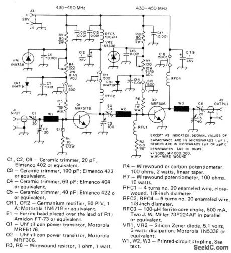
Suitable for mak-ing DX contacts through Oscar satellite, as well as for tropo and local contacts, using CW or SSB. Motorola MRF5176 transistor provides drive to MRF306 output stage, giving sufficient output over range of 430-450 MHz. Requires 1-3 W RF input. Microstrip conductors W1-W3, each 0.077 wavelength long, provide wideband matching and high efficiency. Article gives dimensioned layout for printed-circuit board and all construction details.-J. Buscemi, A 60-Watt Solid-State UHF Linear Amplifier, QST, July 1977, p 42-45. (View)
View full Circuit Diagram | Comments | Reading(698)
EMI_FREE_PHASE_CONTROL_OF_HEATER
Published:2009/7/8 3:08:00 Author:May
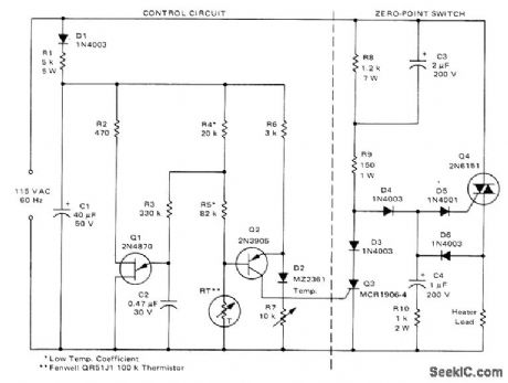
Modulated triac zero-point switch eliminates electromagnetic interference generated by phase control while providing proportional ON/ OFF switching for accurate temperature regulation of heater load. Circuit at right of dashed line is basic zero-point switch that tums triac on almost immediately after each zero crossing between half-cycles. R7 is set so bridge in control circuit is balanced at desired temperature.When temperature overshoots, thermistor RT decreases in resistance and Q2 tums on to providegate drivefor SCR Q3. Q3 then tums on and shunts gate signal away from triac Q4, to remove power from load. When temperature drops, Q2 and Q3 tum off and full-wave power is applied to load. Modulation is achieved by supelimposing sawtooth voltage from Q1 on one arm of bridge through R3, With sawtooth period equal to 12 cycles ol line frequency. From 1 to 12 of these cycles can be applied to load for modulating power in 8% steps from 0% to 100% duty cycle.- Circuit Applications for the Triac, Motorola, Phoenix, AZ, 1971, AN-466, p 13. (View)
View full Circuit Diagram | Comments | Reading(733)
75℃_CRYSTAL_OVEN
Published:2009/7/8 2:59:00 Author:May
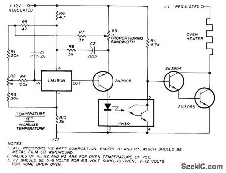
Proportional temperature controller using National LM3911 IC holds crystal oven temperature constant within 0.1℃ of 75 ℃, to improve stability of oscillator used in frequency synthesizers and digital counters.Duty cycle of square-wave output of IC (ratio of OFF to ON time) varies with temperature of sensol in IC and with voltage at inverting input ter-minal. Duty cycle change makes average heater current change as required to bring temperature back to desired value. Square-wave frequency is determined by R4 and C1. 4N30 optocoupler drives power transistor having oven heater in collector circuit. During ON intervals of square wave, power transistor is driven to saturation, and during OFF intervals is cut off.-F. Schmidt, Precision Temperature Control for Crystal Ovens, Ham Radio, Feb. 1978, p 34-37.
(View)
View full Circuit Diagram | Comments | Reading(1537)
ONE_SHOT_TIMER
Published:2009/7/8 2:58:00 Author:May
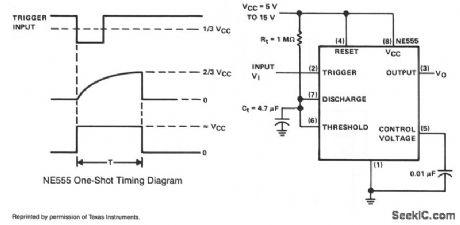
This simple circuit consists of only two timing components RTand CT, the NE555, and bypass capacitor C2. While not essential for operation, C2 is recommended for noise immunity. During standby, the trigger input terminal is held higher than 1/3 VCC and the output is low. When a trigger pulse appears with a level less than 1/3 VCC, the timer is triggered and the timing cycle starts. The output rises to a high level near VCC, and at the same time, CT begins to charge toward VCC. When the CT vottage crosses 2/3 VCC, the timing period ends with the output falling to zero, and the circuit is ready for another input trigger. Because of the internal latching mechanism, the timer will always time out when triggered, regardless of any subsequent noise, such as bounce, on the trigger input. For this reason, the circuit can also be used as a bounceless switch by using a shorter rc time constant. A 100-KΩ resistor for RT and a 1-μF capacitor for CT would give a clean, 0.1 s output pulse when used as a bounceless switch. (View)
View full Circuit Diagram | Comments | Reading(871)
455_kHz_SECOND_IF_
Published:2009/7/8 2:54:00 Author:May
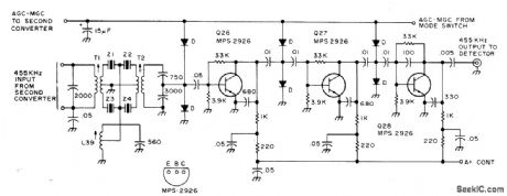
Used in all-band doubleconversion superheterodyne receiver for AM,narrow-band FM, CW, and SSB operation. Input is fed through 455-kHz ceramic filter to highgain amplifier using three MPS 2926 transistors all having automatic gain control and master gain control. Use of silicon rectifiers in interstage networks of IF amplifier gives economical wide-range AGC circuit Supρlγ;is13.6 V regulated Article gives all circuits of receiver.-DM.Eisenberg,Build This All-Band VHF Receiver,73 Magazine,Jan 1975,p 105-112. (View)
View full Circuit Diagram | Comments | Reading(6497)
SIMPLE_TIME_DELAY
Published:2009/7/8 2:23:00 Author:May
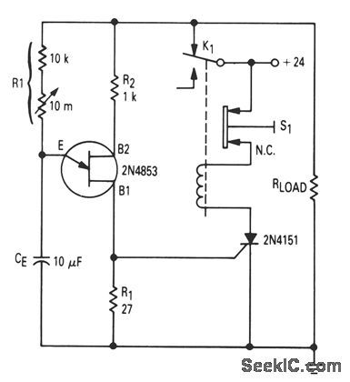
After the first cycle, the relay will normally be energized. When normally closed pushbutton S1 is activated, the SCR turns off, the relay is de-energized, and power is applied to the relaxation oscilla-tor and the load. After a time delay varying from less than a second to approximately 2.5 minutes, as determined by the setting of the 10-MΩ potentiom-eter, the unijuction will fire and turn on the SCR. The relay will energize until power is removed from the oscillator and the load, and will stay energized until button S1 is pushed again. The UJT trigger output from base 1 directly drives the gate of the SCR. However, where isolation between the UJT trigger or any other type of trigger and the thyristor power circuit is required, then a simple pulse trans-former, interfacing the two elements, will suffice. (View)
View full Circuit Diagram | Comments | Reading(2803)
TIMING_THRESHOLD_AND_LOAD_DRIVER
Published:2009/7/8 2:20:00 Author:May
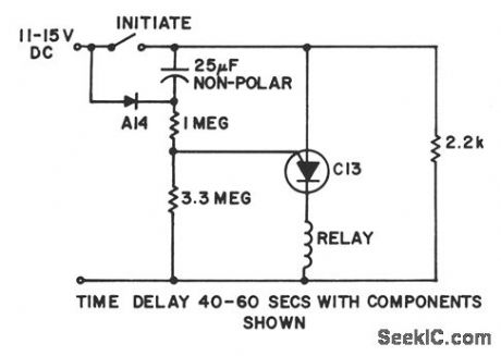
Power is applied to the circuit with the initiate switch open. The 25-μF capacitor charges through the A14, or equivalent, diode and 2.2-KΩ resistor to full supply voltage. When the initiate switch is closed, the low side of the capacitor is suddenly raised to + 12 V. This raises the diode side of the capacitor to approximately +24 V. The capacitor immediately begins discharging through the seriesconnected 1 and 3.3-MΩ resistors. Eventually, the C13 gate becomes forward biased, the device tums, and it applies power to the relay. The delay is virtually independent of supply voltage. (View)
View full Circuit Diagram | Comments | Reading(587)
_ELECTRONIC_TIME_DELAY
Published:2009/7/8 2:18:00 Author:May
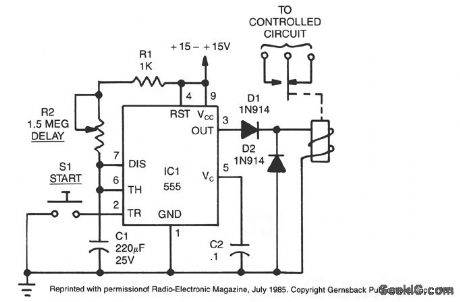
The time delay, T', in seconds is: T = 1.1 x C1 x (R1 + R2). The resistances are in megohms and capacitances in microfarads. The sum of R1 and R2 should not be less than 1000 Ω nor higher than 20 MΩ. Pressing S1 starts the timing cycle. A low-going pulse, instead of S1 can also be used to initiate the timing cycle. With the values shown and allowing for the tolerances of the 200-μF capacitor, the delay will range from 4 minutes and 50 seconds to 7 minutes and 26 seconds. The output terminal, pin 3, of 555, is normally low and switches high during the timing cycle. The output can either sink or source currents up to 200 mA. Therefore, a load such as a relay coil can be connected between pin 3 and VCC or between pin 3 and ground, depending on circuit requirements. When the relay is connected between pin 3 and ground, it is normally de-energized so it is energized only during the timing cycle. Connecting the relay to ground will save power and allow the IC to run cool. (View)
View full Circuit Diagram | Comments | Reading(655)
PULSE_AMPLITUDE_DISCRIMINATOR
Published:2009/7/8 2:15:00 Author:May
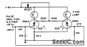
A 1-V amplitude pulse triggers SCS1,but has insufficient amplitude to trigger SCS2.A 3-V mputpulse is delayed h reaching SCS1 by the 10-KΩ and.001-μF integrating network.Instead,it triggers SCS2,then ralses the common emitter voltage to prevent SCS1 from triggering.The 100-KΩ resistors Suppress the rate effect. (View)
View full Circuit Diagram | Comments | Reading(1)
CLOSED_LOOP_TRACER
Published:2009/7/8 2:13:00 Author:May
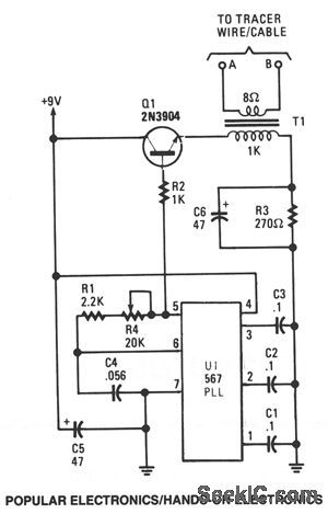
The tracer, consisting of both a transmitter and receiver, is designed to follow a closed-loop wire or cable system. It follows an induced voltage path created by feeding a low-current, audio-frequency signal through the cable. When the pick-up coils come within close proximity of the current-carrying cable, a small voltage is generated in each coil, and that induced voltage is then processed by the receiver's circuitry.
The circuit is built around a 567 phase-locked loop (PLL) configured as a variable-frequency, audio-generator circuit, which is designed to produce a square-wave output at pin 5. Potentiometer R4 allows the oscillator to be easily tuned to the receiver's frequency. Transistor Q1 isolates the oscillator from the load and matches the impedance of the primary of T1. Resistor R3 limits current flow through Q1. The low-impedance secondary of T1 supplies the cable drive signal. (View)
View full Circuit Diagram | Comments | Reading(3398)
DOWNBEAT_EMPHASIZED_ELECTRONIC_METRONOME
Published:2009/7/8 2:12:00 Author:May
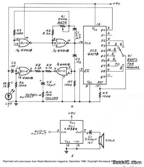
IC1a and IC1b form an astable multivibrator. The astable's signal is fed to IC1c, also to the clock input of IC2, a 4017B decade counter. That IC's Q0 through Q9 outputs become high one at a time for each successive clock pulse received at pin 14. Switch S1 feeds one of those outputs to the 4017B's reset input. Whenever the selected output becomes high, the 4017B restarts its counting cycle; that determines the number of beats per measure. The network composed of C2 and R6 sharpens the downbeat pulse, and the network composed of C3 and R7 sharpens the free-running pulses. By making C2 larger than C3, the downbeat receives greater emphasis.
(View)
View full Circuit Diagram | Comments | Reading(596)
CONSTANT_CURRENT_STIMULATOR
Published:2009/7/8 2:10:00 Author:May
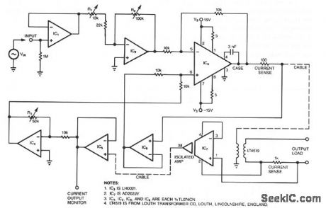

Most circuits that provide an electrical stimulus for research subjects are constant-voltage designs; this circuit is a constant-current design. Stimulator circuits must be isolated for two reasons: to ensure safety and to minimize interference. Isolated stimulators are essentially two-terminal devices; output currents can flow only between the two output terminals and can at no time flow through any other path, such as the power ground.
The circuit's bandwidth ranges from 50 Hz to 5 kHz when a ± 1 V sinusoidal input drives the circuit.Output loads can range from a short circuit to 100 KΩ and have as much as 0.033 μF of parallel capacitance. The transformer and associated circuitry conveniently connect to the main circuit via a cable. Note: This circuit is not approved for use on human beings.
Op amps, IC1 and IC2, buffer and set the gain of the circuit, respectively. You adjust trimmer R1 so that R2, a 10-turn pot, yields output currents ranging from 0 to 1 mA/VIN. IC3 is a power op amp. Its output drives the primary of a transformer that has a current gain of 0.1, or avoltage gain of10. Operating from a + 15 V supply, the transformer therefore has a voltage compliance of ±150 V.
The circuit senses not only the current supplied to the transformer but also the current in the transformer's secondary. IC7, a fully isolated, medical-grade amplifier, provides the isolated feedback signal because the op amp has its own built-in isolation transformer. Trimmer R3 sets the feedback gain precisely at 27 KΩ nominal. (View)
View full Circuit Diagram | Comments | Reading(1340)
STIMULUS_ISOLATOR
Published:2009/7/8 2:09:00 Author:May
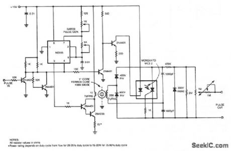
This stimulus isolator uses a photo-SCR and a toroid for shaping pulses of up to 200 V at 200μA.
(View)
View full Circuit Diagram | Comments | Reading(581)
| Pages:237/471 At 20221222223224225226227228229230231232233234235236237238239240Under 20 |
Circuit Categories
power supply circuit
Amplifier Circuit
Basic Circuit
LED and Light Circuit
Sensor Circuit
Signal Processing
Electrical Equipment Circuit
Control Circuit
Remote Control Circuit
A/D-D/A Converter Circuit
Audio Circuit
Measuring and Test Circuit
Communication Circuit
Computer-Related Circuit
555 Circuit
Automotive Circuit
Repairing Circuit