
Index 231
ELECTRONIC_DOOR_BUZZER
Published:2009/7/8 22:52:00 Author:May
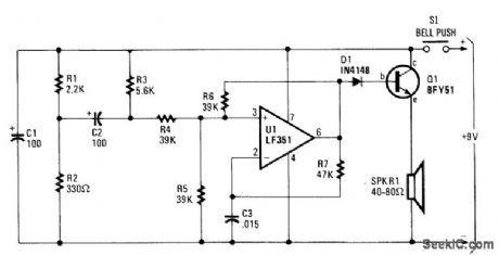
When S1 is depressed, an initial positive voltage is placed on C2 and the noninverting terminal of U1.The circuit oscillates at a low frequency. As C2 charges up through R3, a rapid increase in frequency of oscillation results, producing (at SPKR1) a rapidly rising pitched sound. This sound is easily recognized over ambient noise. (View)
View full Circuit Diagram | Comments | Reading(1588)
_OPTICAL_TTL_COUPLER
Published:2009/7/8 22:49:00 Author:May
For higher speed applications, up to 1-MHz NRZ, the Schmitt-trigger output H11L series optoisolator provides many features. The 1.6-mA drive current allows fan-in circuitry to drive the IRED, while the 5-V, 270-Ω sink capability and 100-ns transition times of the output add to the logic coupling flexibility. (View)
View full Circuit Diagram | Comments | Reading(839)
HIGH_GAN_FOR_WEAK_SIGNALS
Published:2009/7/8 22:46:00 Author:May
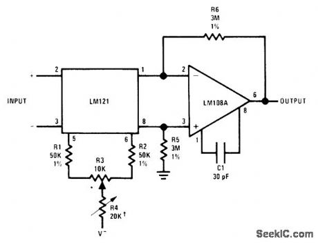
NationaI LM121 differential amplifier is operated openloop as input stage for input signals up to ±10 mV. Input voltage is converted to differential output current for driving opamp acting as current-to-voltage converter with single-ended output. R4 is adjusted to set gain at 1000. Null pot R3 serves for offset adjustment. - Linear Applications, Vol, 2, National Semiconductor, Santa Clara, CA, 1976, AN-79, p 7-8. (View)
View full Circuit Diagram | Comments | Reading(691)
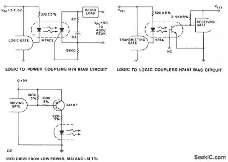
OPTICAL_CMOS_COUPLER
Published:2009/7/8 22:46:00 Author:May


required current to the IRED if CMOS is to drivethe optocoupler.As in the case of the low output TTL families,the H74A output can drive a multiplicity of CMOS gate inputs or a standard TTL input given the proper bias of the IRED. A onelogic stage drives the IRED on. This circuit will provide worst-case drive criteria to the IRED for logic supply voltages from 3 to 10 V, although lower power dissipation can be obtained by using higher value resistors for high supply voltages. If this is desired, the worst-case drive must be supplied to the IRED with minimum supply voltage, minimum temperature and maximum resistor tolerances, gate saturation resistance, and transistor saturation voltages applied. For the H74 devices, minimum IRED current at worst-case conditions, zero logic state output of the driving gate, is 6.5 mA and the H11L1 is 1.6 mA. (View)
View full Circuit Diagram | Comments | Reading(688)
AD_BOARD
Published:2009/7/8 22:44:00 Author:May

An IBM PC can operate the two 12-bit A/D converters in Fig. 1 via its printer port. The converters' serial outputs use only two of the printer port's eight data lines (DATA A OUT, DATA B OUT). Because the IBM PC's printer port supplies no power, interface software running on the PC programs the six unused data lines high. Busing these data lines provides power for the digital portion of the A/D con-verters. (The converters have internal optoisolators. Consequently, you must provide isolated supplies for their analog sides.)
Although the converters can execute 12-bit conversions in 6 μs, the slow software-driven approach used in this Design Idea stretches conversion periods out to about 100 μs (depending on your PC's clock speed).
The circuit takes advantage of the converters' optoisolator inputs to put their clock and start inputs in series. Therefore, the converters operate synchronously.
The accompanying software starts the conversions, issues clock pulses, reads the data bits as they become available, and stores them in memory. The listing is too long to reproduce here; you can obtain it from the EDN BBS (617-558-4241, 2400, 8, N, 1). (View)
View full Circuit Diagram | Comments | Reading(781)
FAST_RESPONSESETTLINGLOW_PASS_FILTER
Published:2009/7/8 22:44:00 Author:May
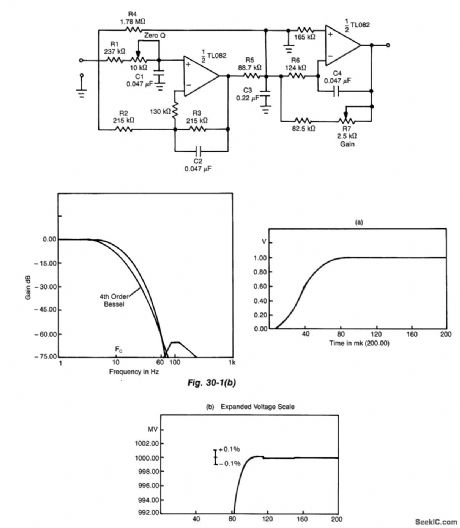
This circuit uses a Wien Bridge and variable negative feedback. R7 controls the gain and R8A and R8B controls the tuned frequency. (View)
View full Circuit Diagram | Comments | Reading(735)
NORMALLY_CLOSED_HALF_WAVE_zvs_CONTACT_CIRCUIT
Published:2009/7/8 22:39:00 Author:May

A normally closed contact circuit that provides zero-voltage switching is designed around the 4N39 SCR optocoupler. The circuit illustrates the method of modifying the normally open contact circuit by using the photo SCR to hold off the trigger SCR. (View)
View full Circuit Diagram | Comments | Reading(1397)
WIDEBAND_ACTIVE_ROD_ANTENNA
Published:2009/7/8 22:36:00 Author:May
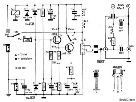
A J309 Siliconix FET feeds a 2N5109 in a wideband RF amplifier configuration. A relay is used to bypass the amplifier in the transmit mode (if desired). A 2-m 5/8-wave whip is used as the active antenna element. The amplifier is fed dc via the coax cable, which makes the use of only a single coax lead for both signal and power. U1 is a surge arrester for electrostatic discharge protection. (View)
View full Circuit Diagram | Comments | Reading(2807)
AUTOMATIC_CALIBRATOR
Published:2009/7/8 22:36:00 Author:May
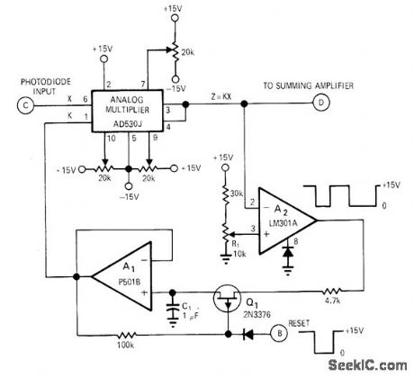
Automatic scaling circuit permits frequent and fast recalibration for precision optical measurements, to compensate for variations in light intensity due to thermal cycling of lamp filament, dirty optics, and gain variations between photodetectors and between amplifiers. With reset pulse at point B, comparator A2 compares output of multiplier to preset reference voltage on R1. If A2 input voltage is greater than reference applied to pin 3 by R2, output switches to zero and remains there until C1 has discharged enough to lower output of A1 and output of multiplier below reference on pin 3. If input at pin 2 ofA2 is less than reference on pin 3,A2 will switch to 15 V and output of multiplier will be adjusted upward until voltage on pin 2 of A2 again exceeds that on pin 3. Output of A2 is thus continually switching between 15 V and 0 V during reset or scaling. After reset pulse is removed, scale factor K is maintained constant by multiplier during measuring.-R. E. Keil, Automatic Scaling Circuit for Optical Measurements, EDN/EEE Magazine, Nov. 15, 1971, p 49-50. (View)
View full Circuit Diagram | Comments | Reading(656)
WIRELESS_FM_MICROPHONE_1
Published:2009/7/8 22:31:00 Author:May
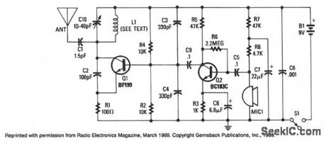
Adjustable capacitor C10, and coil L1 form a tank circuit that, in combination with Q1, C2, and R1, oscillates at a frequency on the FM band. The center frequency is set by adjusting C10. An electret microphone, M1, picks up an audio signal that is amplified by transistor Q2. The audio signal is coupled via C9 to Q1, which frequency modulates the tank circuit. The signal is then radiated from the antenna. The circuit can operate from 9-12 Vdc. (View)
View full Circuit Diagram | Comments | Reading(1137)
ACTIVE_ANTENNA_Ⅱ
Published:2009/7/8 22:31:00 Author:May
This circuit provides 14-to 20-dB gam at frequencies from 10 kHz to 30 MHz.The antenna length canbe anything between 5 and 10 feet.A 102-inch CB whip is excellent for this purpose. (View)
View full Circuit Diagram | Comments | Reading(776)
ACTIVE_ANTENNA_I
Published:2009/7/8 22:28:00 Author:May
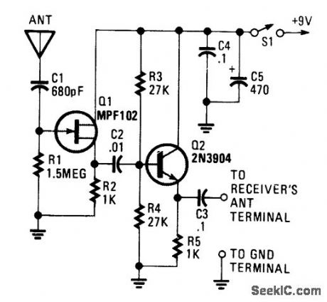
This circuit is designed to make a short pull-up antenna perform like a long wire antenna, while offering no voltage gain. The circuit boosts the receiver's performance only if the signal at the antenna is of sufficient level to begin with.
This circuit takes a short pull-up antenna that has a high output impedance and couples it to the receiver's low input impedance through a two-tran-sistor impedance-matching network. Transistor Q1's high input impedance and high-frequency characteristics make it a good match for the short antenna, and Q2's low output impedance is a close match for the receiver's input. This circuit is usable over the range from 100 kHz to 30 MHz. (View)
View full Circuit Diagram | Comments | Reading(1356)
VHF_MODULATOR
Published:2009/7/8 22:28:00 Author:May
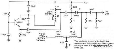
This circuit uses an oscillator (2N2222) and a diode D1 as a nonlinear mixer. The frequency is set by a slug in L1. RFC1, C1, and RFC2 form a low-pass filter to pass video and block rf from the video source. (View)
View full Circuit Diagram | Comments | Reading(1319)
TRIGGERING_SCR_SERIES
Published:2009/7/8 22:27:00 Author:May

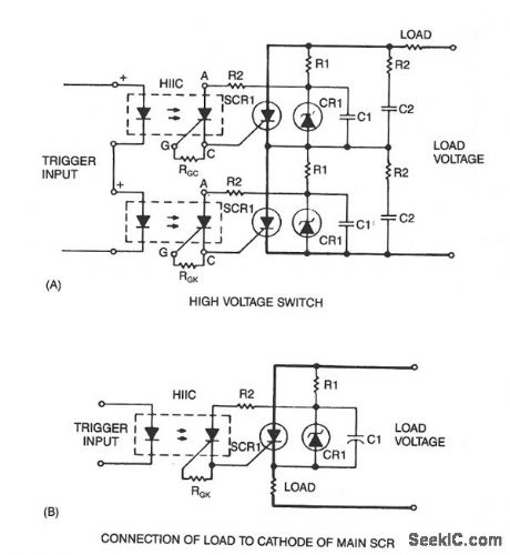
Snubber circuit R2C2, as shown, might be necessary since RI and C1 are tailored for optimized triggering and not for dV/dt protection. Fiber-optic pairs can be used with discrete SCRs to switch thousands of volts. A photon coupler with a transistor output will limit the trigger-pulse amplitude and rise time because of CTR and saturation effects. Using the H11C1, the rise time of the input pulse to the photon coupler is not critical, and its amplitude is limited only by the H11C1 turn-on sensitivity. The load can also be connected to the cathode as illustrated in Fig. 67-3B. (View)
View full Circuit Diagram | Comments | Reading(749)
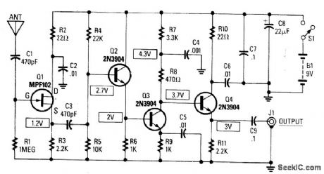
ACTIVE_ANTENNA_WITH_GAIN
Published:2009/7/8 22:20:00 Author:May
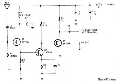
The signal boostei,built around a few transistors and support components,offers an RF galn of about12 to 18 dB (from about 100 kHz to over 30 MHz).
The RF signal is direct-coupled from Q1’s Source terminal to the base of Q2,which is configured as avoltage amplifier. The output of Q2 is then direct-coupled to the base of Q3 (configured as an emitter-fallower amplifier).Transistor Q3 is used to match and isolate the gam stage from the receiver’s RF-inputcircuitry.
Inductor L1 is used to keep any power Source nolse from reaching the FET (Q1) and any value of RF choke from 0.5 to 2.5 mH will do.The value of R2 sets the Q2 bias at about 2V. If the voltage is less than 2V, Increase the value of R2 to 1.5 kΩ,To go below 100 kHz(to the bottom ofthe RF spectrum),increasethe value of C1 to 0.002 μF. The antenna is a short pull-up type (42″to 86″long). (View)
View full Circuit Diagram | Comments | Reading(758)
DIGITAL_ENTRY_LOCK
Published:2009/7/8 22:15:00 Author:May
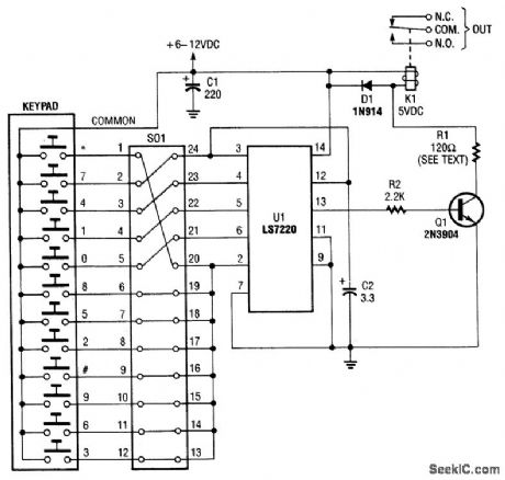
A keypad enters a four-digit access code, which is programmed via jumpers on a 24-pin plug-in header and socket. U1 is an LST220, which detects a four-digit sequential data input. When the correct data is entered into the keyboard, pin 13 of U1 goes high, which activates Q1 and K1. K1 drives an external electric lock solenoid, etc. (View)
View full Circuit Diagram | Comments | Reading(1742)
_HIGH_Q_NOTCH_FILTER
Published:2009/7/8 22:10:00 Author:May


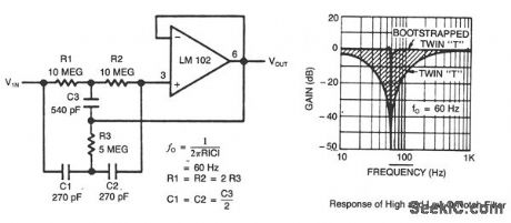
This circuit shows a twin-T network connected to an LM102 to form a high-Q, 60-Hz notch filter. The junction of R3 and C3 which is normally connected to ground, is bootstrapped to the output of the follower.Because the output of the follower is a very low impedance, neither the depth nor the frequency of the notch change ; however, the Q is raised in proportion to the amount of signal fed back to R3 and C3. Shown is the response of a normal twin-T and the response with the follower added.
(View)
View full Circuit Diagram | Comments | Reading(966)
TWIN_T_NOITCH_FILTER
Published:2009/7/8 22:09:00 Author:May
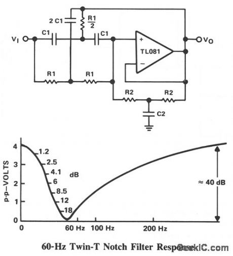
This filter is used to reject or block a frequency or band of frequencies. These filters are often designed into audio and instrumentation systems to eliminate a single frequency, such as 60 Hz. Commercial grade components with 5%-1070 tolerance produce a null depth of at least 30 to 40 dB. When a twin-T network is combined with a TL081 op amp in a circuit, an active filter can be implemented. The added resistor capacitor network, R2 and C2, work effectively in parallel with the original twin-T network, on the input of the filter. These networks set the Q of the filter. The op amp is basically connected as a unity-gain voltage follower. The Q is found from:
R2 C1 Q = — = — 1R2 C2For a 60-Hz notch filter with a @ of 5, it is usually best to pick the C1 capacitor value and calculate the resistor R1. Let C1 = 0.22 μF. Then:
R1 = 12 KΩ R1 = 120 KΩ C2 = 0.047/μF
Standard 5% resistors and 10% capacitors produce a notch depth of about 40 dB, as shown in the frequency response curve.
(View)
View full Circuit Diagram | Comments | Reading(1007)
WIRELESS_FM_MICROPHONE
Published:2009/7/8 22:08:00 Author:May

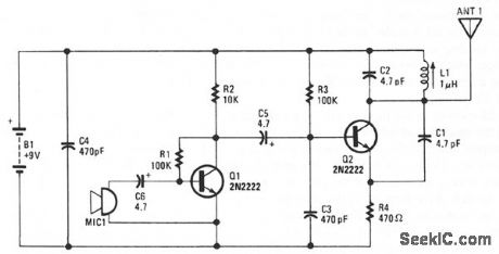
Transistor Q1 acts as an amplifier for condenser microphone MIC1. The output of Q1 is applied to the base of transistor Q2 through a 4.7- μF capacitor. C2 and L1 form an LC tank circuit, which is used to set the frequency at which the transmitter operates. Coil L1 is a variable inductor, centered a bit below 1 μH, that is used to adjust the modulating frequency of the circuit. Capacitors C1 and C2 are 4.7 pF units. A lower value can be used to raise the circuit's operating frequency. The microphone and Q1 provide a vary-ing voltage at the base of Q2, with the output of Q2 applied to the LC tank circuit. That causes a modulating action in the tank circuit that, when applied to the antenna, a short piece of wire 6- to 8-inches long, will provide a good, clear FM signal somewhere in the range of 88 to 95 MHz with a range of about 100 feet. (View)
View full Circuit Diagram | Comments | Reading(1014)
OPAM_PICOAMMETER
Published:2009/7/8 22:05:00 Author:May
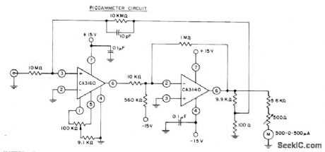
Current-to-voltage converter connection for CA3160 and CA31400 bipolar MOS opamps provides full-scale meter deflection for ±3 pA CA3160 is operated in guarded mode to reduce leakage current.CA3140 provides gain of 100 for driving zerocenter microammeter. With suitable switching, full-scale current ranges of 3 pA to 1 nA can be handled with single 10.000-megohm resistor in overall feedback path.-″Circuit Ideas for RCALinear ICs″RCA Solid State Division Someville,NJ,977,ρ 14. (View)
View full Circuit Diagram | Comments | Reading(1268)
| Pages:231/471 At 20221222223224225226227228229230231232233234235236237238239240Under 20 |
Circuit Categories
power supply circuit
Amplifier Circuit
Basic Circuit
LED and Light Circuit
Sensor Circuit
Signal Processing
Electrical Equipment Circuit
Control Circuit
Remote Control Circuit
A/D-D/A Converter Circuit
Audio Circuit
Measuring and Test Circuit
Communication Circuit
Computer-Related Circuit
555 Circuit
Automotive Circuit
Repairing Circuit