
Index 222
DIGITAL_LOGIC_PROBE
Published:2009/7/9 20:33:00 Author:May
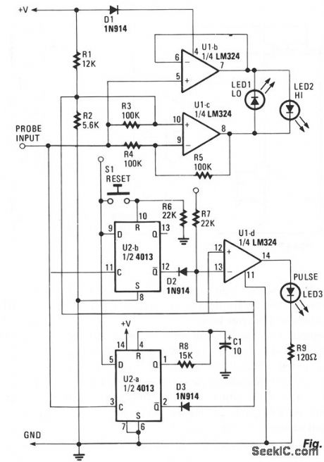
The probe relies on the power supply of the CUT (circuit-under-test). The input to the probe, at probe tip, is fed along two paths. One path flows to the clock inputs of U2a and U2b. The other path feeds both the inverting input of U1c, which is set up as an inverting-mode integrator, and the noninverting input of Ulb, which is configured as a noninverting unity-gain amplifier, in a logic-low state.
That low, below the reference set at pin 10, causes U1b's output at pin 7 to become high. With Ub1 outputting low and U1c outputting high, LED1 is forward-biased, and lights. LED2, reverse-biased, remains dark. Suppose that the logic level on the same pin becomes high. That high is applied to pin 5 of Ulb, causing its output to be high. LED2 is now forward,biased and lights, while LED1 is reverse-biased and becomes dark.
Assume that a clock frequency is sensed at the probe input; LED1 and LED2 alternately light, and depending on the frequency of the signal, can appear constantly lit. That frequency, which is also applied to the clock input of both flip-flops, causes the Q outputs of U2a and U2b to simultaneously alternate between high and low. Each time that the Q outputs of the two flip-flops decrease, the output of U1d increases, lighting LED3, indicating that a pulse stream has been detected. (View)
View full Circuit Diagram | Comments | Reading(1004)
POWER_SUPPLY_BALANCE_INDICATOR
Published:2009/7/9 20:28:00 Author:May
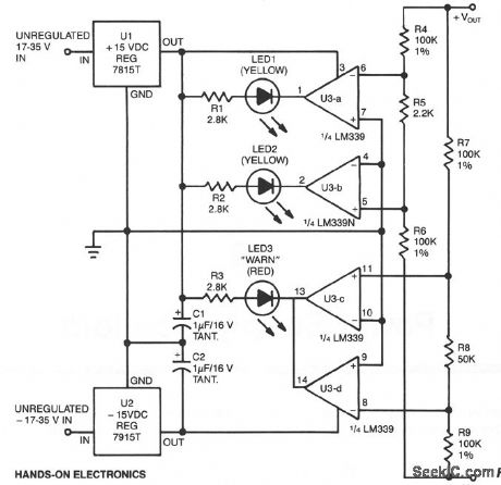
This circuit uses two comparator pairs from an LM339N quad comparator; one pair drives the yellow positive (+) and negative (-) indicators, the other jointly drives the red warn LED3. The circuit draws its power from the unregulated portion of the power supply. The four comparators get their switching inputs from two parallel resistor-divider strings. Both strings have their ends tied between the power supply's positive and negative output terminals. The first string, consisting of R4, R5, and R6, divides the input voltage in half, with output taps at 0.5%. The other string, made up of R7, R8, and R9, also divides the input voltage in half, with taps at + 10%. The 0.5% R4/R5/R6 string drives the two comparators controlling the positive and negative indicators (LED1 and LED2). Their inputs are crossed so that LED2 does not fire until the positive supply is at least 0.5% higher than the negative; the positive indicator does not go off until the negative supply is at least 0.5% higher than the positive-in relative levels. That overlap permits both LEDs to be on when the two supplies are in 1% or better balance. The + 10T R7/R8/R9 string drives the other two comparators, which control the warn indicator. If either side of the supply is 10% or more higher than the other, one of the two comparators will switch its output low and light the red LED3-the LM339N has opened-collector outputs, allowing such wired OR connections. The inputs are not crossed, as with the other comparator pair, so there is a band in the middle where neither comparators output is low and the LED remains off. (View)
View full Circuit Diagram | Comments | Reading(2661)
WIRELESS_IR_SECURITY_SYSTEM
Published:2009/7/9 20:20:00 Author:May
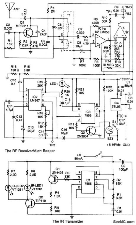
This system contains an IR transmitter, an IR receiver/RF transmitter, and an RF receiver/alert beeper. Two IR LEDs in the transmitter transmit a pulsed beam of invisible infrared light to the receiver, which contains an IR phototransistor. The phototransistor detects and amplifies the pulse-modulated IR beam. If the receiver section senses that the IR beam is momentarily interrupted by an object blocking the beam's path, it triggers the transmitter, which outputs a 49.890-MHz carrier that is amplitude-modulated by a 490-Hz tone.
Upon receiving the 490-Hz amplitude-modulated carrier, the RF receiver/beeper unit sounds an alarm that alerts the user to the intrusion. The system is not limited to just one RF transmitter. A single RF receiver/beeper can be used to monitor any number of RF transmitters (or locations). However, the receiver/beeper unit cannot discriminate between different transmitter sites in multiple-transmitter systems. (View)
View full Circuit Diagram | Comments | Reading(2188)
FEEDBACK_OPAMP_FOR_BRIDGE
Published:2009/7/9 5:55:00 Author:May
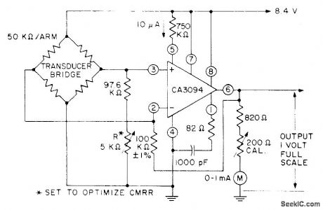
Uses CA3094 programmable opamp to convert differential input signal from resistor bridge to single-ended 1-V output signal. Circuit provides feedback for opamp. RC network between terminals 1 and 4 of opamp provides compensation to improve stability. - Circuit Ideas for RCA Linear ICs, RCA Solid State Division, Somerville, NJ, 1977, p 13. (View)
View full Circuit Diagram | Comments | Reading(636)
IR_RECEIVER_II
Published:2009/7/9 5:51:00 Author:May
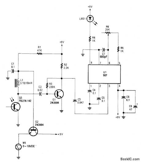
Q3 is an IR phototransistor that responds to a modulated IR beam. Q1 amplifies the ac component of the IR beam. Q2 drives a meter as a relative indication of the strength of the light beam. A strong beam gives a lower meter reading. U1 is a tone decoder that produces a low output on pin 1 during reception for an IR beam that is modulated with the correct tone frequency, determined by R6. (View)
View full Circuit Diagram | Comments | Reading(1094)
PLL_DETECTOR_FOR_ALL_METALS
Published:2009/7/9 5:46:00 Author:May
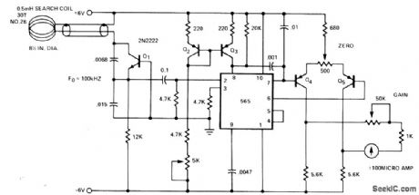
Frequency change produced in Colpitts oscillator by metal object near tank coil is indicated by 565 PLL connected asfrequency meter. Oscillator frequency increases when search coil is brought near nonferrous metal object. Oscillator frequency decreases, as indicated by lower meter reading, when coil is brought nearferrous object.-Signetics Analog Data Manual,''Signetios,Sunnyvale,CA,1977,p 856-858. (View)
View full Circuit Diagram | Comments | Reading(4495)
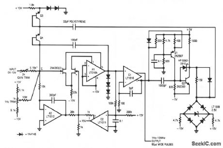
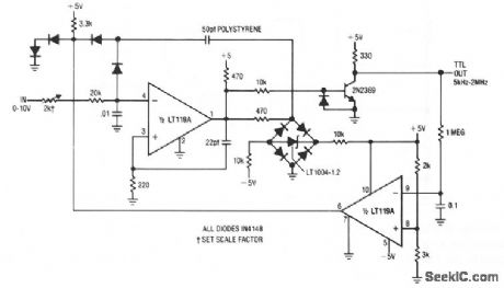
1_HZ_TO-125_MHZ_VOLTAGE_TO_FREQUENCY_CONVERTER
Published:2009/7/9 5:46:00 Author:May
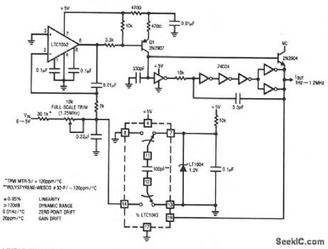
This stabilized voltage-to-frequency converter features 1 Hz-1.25 MHz operation, 0.05% linearity, and a temperature coefficient of typically 20 ppm/°C. This circuit runs from a single 5-V supply. The converter uses a charge feedback scheme to allow the LTC1052 to close a loop around the entire circuit, instead of simply controlling the offset. This approach enhances linearity and stability, but introduces the loop's settling time into the overall voltage-to-frequency step-response characteristic.
(View)
View full Circuit Diagram | Comments | Reading(733)
IR_RECEIVER_I
Published:2009/7/9 5:44:00 Author:May

This receiver is built around a μPC1373 IR remote-control preamplifier, a sensitive 30-to-40 kHz tuned detector, an autoniatic gain control, a peak detector, and an output waveshaping buffer. The demod-ulated signal from the preamp stage is sent to IC4A, a 74C14 Schmitt trigger. The squared-up 1 500-Hz signal is then sent to the clock input of IC5A, half of a 4013 dual D flip-flop. That 750-Hz signal is clipped to approximately 0.7-V p-p by diodes D3 and D4. The clipped signal is then fed to IC6, a 567 tone decoder. The output of that IC goes low whenever the frequency of the signal fed to it is within the lock range of its internal VC0.
When IC6 detects a signal of the proper frequency, pin 8 goes low. The output signal is fed through another Schmitt trigger (IC4B), which drives another D flip-flop, IC5B. Schmitt trigger IC4B also drives IC4C, which in turn drives LED4, SIGNAL, which fights up whenever a signal is received. The Q output of IC5B drives two parallel-connected inverters. IC4C and IC4F turn transistor Q2 on when Q goes low. That transistor energizes the relay; its contacts switch the controlled device on and off. (View)
View full Circuit Diagram | Comments | Reading(934)
VOLTAGE_TO_FREQUENCY_CONVERTER
Published:2009/7/9 5:42:00 Author:May
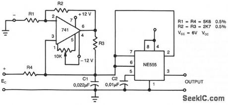
This circuit can accept positive or negative or differential control voltages. The output frequency is zero when the control voltage is zero. The 741 op amp forms a current source controlled by the voltage EC to charge the timing capacitor C1 linearly. NE555 is connected in the astable mode, so that the capacitor charges and discharges between 1/3 VCC and 2/3 VCC. The offset is adjusted by the 10-K potentiometer so that the frequency is zero when the input is zero. For the component values shown: f≈ 4.2 EC kHz. If two dc voltages are applied to the ends of R1 and R4, the output frequency will be proportional to the difference between the two voltages. (View)
View full Circuit Diagram | Comments | Reading(3439)
IR_RECEIVERI
Published:2009/7/9 5:39:00 Author:May
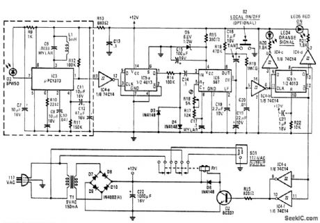
This receiver is built around a μPC1373 IR remote-control preamplifier, a sensitive 30-to-40 kHz tuned detector, an autoniatic gain control, a peak detector, and an output waveshaping buffer. The demod-ulated signal from the preamp stage is sent to IC4A, a 74C14 Schmitt trigger. The squared-up 1 500-Hz signal is then sent to the clock input of IC5A, half of a 4013 dual D flip-flop. That 750-Hz signal is clipped to approximately 0.7-V p-p by diodes D3 and D4. The clipped signal is then fed to IC6, a 567 tone decoder. The output of that IC goes low whenever the frequency of the signal fed to it is within the lock range of its internal VCO.
When IC6 detects a signal of the proper frequency, pin 8 goes low. The output signal is fed through another Schmitt trigger (IC4B), which drives another D flip-flop, IC5B. Schmitt trigger IC4B also drives IC4C, which in turn drives LED4, SIGNAL, which fights up whenever a signal is received. The Q output of IC5B drives two parallel-connected inverters. IC4C and IC4F turn transistor Q2 on when Q goes low. That transistor energizes the relay; its contacts switch the controlled device on and off. (View)
View full Circuit Diagram | Comments | Reading(727)
PORTABLE_NICAD_CHARGER
Published:2009/7/9 5:36:00 Author:May
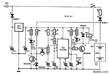
The portable charger is intended primarily to give model enthusiasts the opportunity of charging their Nicad batteries from a car battery out in the open. The supply voltage for the circuit is regulated by IC1.
When the circuit is connected to the car battery, D2 lights only if the Nicad to be charged has been connected with correct polarity. For that purpose, the + terminal of the Nicad battery is connected to the base of T1 via R8. Because even a discharged battery provides some voltage, T1 is switched on and D2 lights.
Only if the polarity is correct will the pressing of the start switch, S1, have any effect. If so, the collec-tor voltage of T1 is virtually zero so that monostable IC2 is triggered by S1. The output, pin 3, of this CMOS timer then becomes high, T2 is switched on and relay Re1 is energized. Charging of the Nicad battery, via R5 and D6, then begins and charging indicator D4 lights. During the charging, C4 is charged slowly via P1 and R4. The.value of these components determines the mono time of IC2 and thus the charging period of the Nicad battery. With values as shown in the diagram, that period can be set with P1 to between 26 and 33 min. Notice that this time is affected by the leakage current of C4; use a good-quality capacitor here. The charging can be interrupted with reset switch S2.
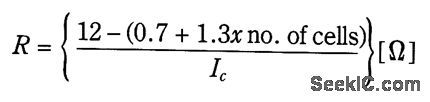
The charging current through the Nicad battery is determined by the value of R, which can be calcu-lated:
IC is the charging current, which is here because the chosen charging period is twice the nominal value of the capacity of the Nicad battery. Resistor R must be able to dissipate a power of IC2RW. Finally, make sure that the Nicad battery is suitable for fast charging; never charge for longer than half an hour! (View)
View full Circuit Diagram | Comments | Reading(758)
PRESERVED_INPUT_VOLTAGE_TO_FREQUENCY_CONVERTER
Published:2009/7/9 5:32:00 Author:May
|The input voltage, V1, causes C1 to charge and produce a ramp voltage at the output of the 741 op amp. Diodes D1 and D2 are four-layer devices. When the voltage across C1 reaches the breakover voltage of either diode, the diode conducts to discharge C1 rapidly and the op amp output goes abruptly to zero. This rapid discharge action applies a narrow pulse to G1 and G2. Positive discharge pulses produced by a positive V1 are coupled to the output only through G1, while negative pulses are coupled only through G2.Because of the forward breakover current of diodes D1 and D2, the circuit won't operate below a minimum input voltage. An increase of R1 increases this minimum voltage and reduces the circuit's dynamic range. The minimum input voltage with R1 at 1 KΩ is in the range of 10 to 50 mV. This input dead zone, when input signal V1 is near zero is desirable in applications that require a signal to exceed a certain level before an output is generated. (View)
View full Circuit Diagram | Comments | Reading(559)
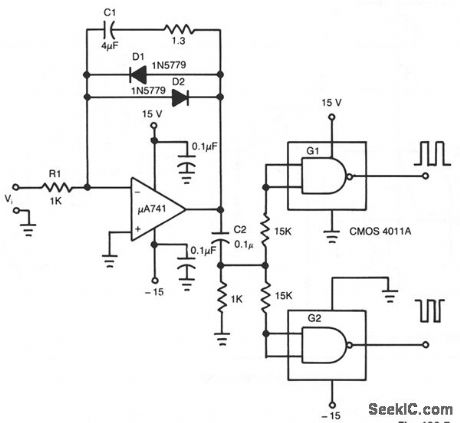
5_kHz_TO_2_MHz_VOLTAGE_TO_FREQUENCY_CONVERTER
Published:2009/7/9 5:28:00 Author:May
View full Circuit Diagram | Comments | Reading(678)
VOLTAGE_REGULATOR_FOR_CARS_AND_MOTORCYCLES
Published:2009/7/9 5:26:00 Author:May
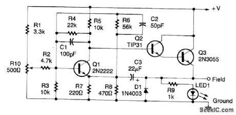
This regulator circuit can be used on an alternator that has one field terminal grounded. When +V (input) gets too high, Q1 conducts, and the base of Q2 is driven toward ground, reducing the voltage fed to Q3. This lowers the voltage fed to the field of the altemator. (View)
View full Circuit Diagram | Comments | Reading(3167)
WINDSHIELD_WIPER_INTERVAL_CONTROLLER
Published:2009/7/9 5:25:00 Author:May
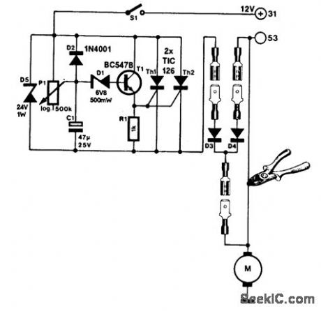
The windshield wiper interval circuit presented here is very compact and is noteworthy for its use of two thyristors, instead of a relay. It has only two connections and operates without any problemseven in conjunction with multistage wiper circuits.
The connecting wire between the wiper motor and terminal S3 is cut and new connections are made (as shown in the diagram). When the interval switch, S1, is closed, capacitor C1 charges via P1 and the wiper motor. After a time set with P1, transistor T1 switches on and triggers the thyristors. The wiper motor is then energized via the thyristors and D3 and sets the wipers into motion. At the same time, C1 discharges via D2 and the thyristors.
After a short time, the wiper stop switch con-nects terminal 53 to the +12-V line so that the wiper motor is energized via D4. The thyristors are switched off because the voltage drop across D3 plus Th1/Th2 is then greater than that across D4. When the wipers reach the end of their travel again, the stop switch connects terminal 53 to ground and enables C1 to charge again. (View)
View full Circuit Diagram | Comments | Reading(1322)
WIDE_RANGE_VOLTAGE_TO_FREQUENCY_CONVERTER_1
Published:2009/7/9 5:21:00 Author:May
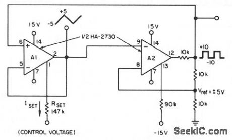
This circuit uses a programmable op amp such as the HA2730-a two-amplifier monolithic chip with independent programming ports for each amplifter-whose slew rate and other parameters vary linearly with a so-called set current. The converter circuit uses one amplifier, A1, as a slewing amplifier and other, A2, as a comparator function. The control voltage VC, determines A1's slew rate. And, because A1's output voltage swing is constant, the modulation of its set current results in direct control of the circuit's frequency. A1's internal compensation capacitor acts as the timing component. An internal bipolar current source,whose current magnitude is directly proportional to the set current of pin 1, then determines the charge-discharge rate. A conversion nonlinearity of ±0.03% of full scale over 3 decades and ±1.5% of full scale over4.3 decades of frequency is possible. The frequency range is adjustable by a change in the resistance R. (View)
View full Circuit Diagram | Comments | Reading(691)
HIGH_CMRR
Published:2009/7/9 5:15:00 Author:May
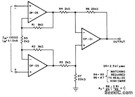
Use of two Precision MonolithIcs OP-05 opamps feeding OP-01 opamp gives input impedance of about 100 gigohms and high common-mode rejection for instrumentationapplications. -'' lnstrumentation Operational Amplifier, Precision Monolithics, Santa Clara, CA, 1977, OP-05, p 7. (View)
View full Circuit Diagram | Comments | Reading(919)
TRANSISTORIZED_BAR_GRAPH_DRIVER
Published:2009/7/9 5:15:00 Author:May
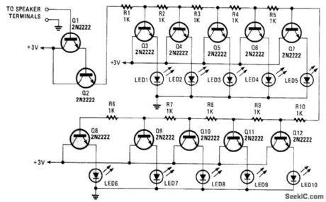
A resistor network (R1 through R10) with emitter followers (Q1 and Q2) drives LED drivers (Q3 through Q7). This circuit was used as a light organ to provide visual volume indication. It can be hooked to a speaker, to another audio source, etc. (View)
View full Circuit Diagram | Comments | Reading(844)
SOLID_STATE_WINDSHIELD_WIPER_DELAY
Published:2009/7/9 5:13:00 Author:May
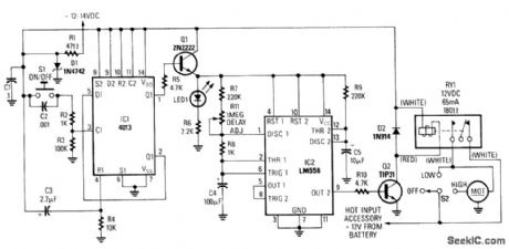
In the wiper-delay schematic shown, with the ignition on, D1 maintains regulated + 12 Vdc. When S1 closes, C1 bypasses transients and passes this + 12 Vdc to divider R2-R3, producing a TTL high at pin 3 of IC1, a 4013 CMOS dual leading-edge triggered D-type flip-flop. Filter R4/C3 keeps IC1 from triggering erroneously when the ignition is on. When S1 is pressed, output Q1 (pin 1) of IC1 latches high, turning on Q1, which conducts via R5, turning on IC2; LED1 indicates power, and R6 sets the current. Because IC2 depends on Q1 for power, IC2 stays off until Q1 turns on.
The left half of IC2 is an astable, with its delay set by R7, R8, R11, and C4. The right half of IC2 is a monostable, with its pulse duration set by R9 and C5. With the values used, you might expect R11 to vary the delay from about 15 to 84 seconds, with a 2.42-second monostable pulse operating the wiper blades on each cycle. However, the actual delay will range between 2 to 18 s, with a 1-s monostable pulse on each cycle. That discrepancy stems from the fact that IC2 is being fed from the emitter of Q1, rather than directly from the regulated +12-V supply. Transistor Q1 acts as an active current source, charges and discharges C4 faster than it ordinarily would.
The astable output (OUT1, pin 5) is tied to TRIG2 (pin 8). When OUT2 (pin 9) becomes high, Q2 is biased via RIO and current flows through RY1, with D2 dissipating back-emf when RY1 shuts off. (View)
View full Circuit Diagram | Comments | Reading(2409)
WIDE_RANGE_VOLTAGE_TO_FREQUENCY_CONVERTER
Published:2009/7/9 5:13:00 Author:May
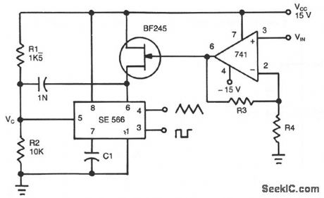
This circuit is based upon the change of frequency of the function generator with the input voltage VIN Generally, the frequency depends upon the capacitance and resistor connected to pin 6. This resistor is replaced by the FET. The frequency range is adjustable by changing the input voltage, VIN; the converter will give a range of 10 Hz to 1 MHz. (View)
View full Circuit Diagram | Comments | Reading(810)
| Pages:222/471 At 20221222223224225226227228229230231232233234235236237238239240Under 20 |
Circuit Categories
power supply circuit
Amplifier Circuit
Basic Circuit
LED and Light Circuit
Sensor Circuit
Signal Processing
Electrical Equipment Circuit
Control Circuit
Remote Control Circuit
A/D-D/A Converter Circuit
Audio Circuit
Measuring and Test Circuit
Communication Circuit
Computer-Related Circuit
555 Circuit
Automotive Circuit
Repairing Circuit