
Index 223
SENSOR_BRIDGE
Published:2009/7/9 5:11:00 Author:May
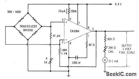
RCA CA3094 combination power switch and amplifier can be used with variety of transducer bridges for instrumentation and other applications. Circuit delivers output of 1 V full-scale for driving meter. Pot R serves as centering or reference control. Can be used as thermometer if one leg of bridge is thermistor and meter scale is calibrated in degrees. -E. M. Noll, Linear IC Principles, Experiments, and Projects, Howard W.Sams, Indianapolis, IN, 1974, p 311-313. (View)
View full Circuit Diagram | Comments | Reading(795)
LOW_COST_VOLTAGE_TO_FREQUENCY_CONVERTER
Published:2009/7/9 5:10:00 Author:May
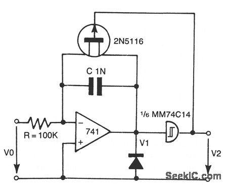
The 741 op amp integrator signal is fed into the Schmitt trigger input of an inverter. When the signal reaches the magnitude of the positive-going threshold voltage, the output of the inverter is switched to zero. The inverter output controls the FET switch directly. For a gate voltage of zero, the FET chan-nel turns on to low resistance and the capacitor is discharged. The discharge current depends on the on resistance of the FET. When the capacitor C1 is discharged to the negative-going threshold voltage level of the inverter, the inverter output is switched to ±12 V. This switch causes the FET channel to be switched off, and the discharging process is switched into a charging process again. Using the components shown, an output frequency of about 10kHZ with 0.1% linearity can be obtained. (View)
View full Circuit Diagram | Comments | Reading(1673)
ADJUSTABLE_10_A_REGULATOR
Published:2009/7/9 5:09:00 Author:May
View full Circuit Diagram | Comments | Reading(639)
TRACKING_PREREGULATOR
Published:2009/7/9 5:08:00 Author:May
View full Circuit Diagram | Comments | Reading(2117)
VARIABLE_VOLTAGE_REGULATOR
Published:2009/7/9 5:07:00 Author:May
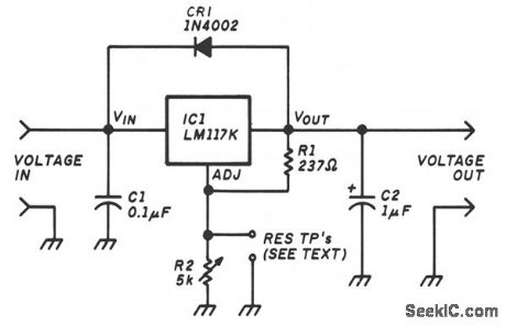
The variable voltage regulator lets you adjust the output voltage of a fixed dc power supply between 1.2 and 37 Vdc, and will supply the output current in excess of 1.5 A. The circuit incorporates an LM117K three-terminal adjustable output positive voltage regulator in a TO-3 can. Thermal overload protection and short-circuit current-limiting constant with temperature are included in the package. Capacitor C1 reduces sensitivity to input line impedance, and C2 reduces excessive ringing. Diode CR1 prevents C2 from discharging through the IC during an output short, (View)
View full Circuit Diagram | Comments | Reading(2917)
LIGHTS_ON_REMINDER_FOR_AUTOS
Published:2009/7/9 5:06:00 Author:May
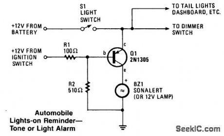

When ignition is off, BZ1 will sound if the head-lights are on. With the ignition on, BZ1 receives no voltage. (View)
View full Circuit Diagram | Comments | Reading(616)
DIFFERENTIAL_INPUT_VARIABLE_GAIN
Published:2009/7/9 5:05:00 Author:May
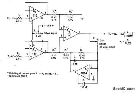
Gainof A3 is varied by modifying feedback returned to R4.A4serves as active attenuator in feedback path presenting constant zero-impedancesource to R4 as required for maintaining goodbalance and high CMRR,With values shown,galn can be varied from unitγ to 300-.W.G.Jung,IC Op-Amp Cookbook,''Howard W,Sams,Indianapolis,IN,1974,ρ 238-239. (View)
View full Circuit Diagram | Comments | Reading(692)
DIFFERENTIAL_INPUT_VOLTAGE_TO_FREQUENCY_CONVERTER
Published:2009/7/9 5:04:00 Author:May
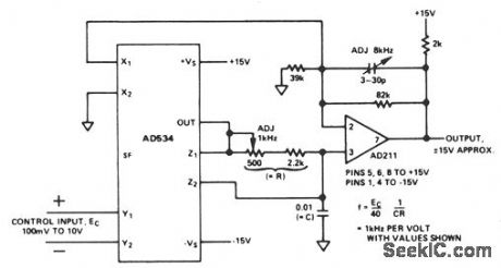
View full Circuit Diagram | Comments | Reading(558)
NIGHT_SAFETΥ_LIGHT_FOR_AUTOS
Published:2009/7/9 5:03:00 Author:May
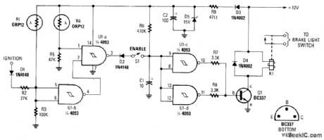
This circuit turns on the brake lights of a parked car when the headlights of an oncoming car are detected, warning the driver of the oncoming car about the parked vehicle. LDR4 is the sensor. LDR1 disables the circuit by causing U1 gate input to be pulled high during daylight hours, causing pin 2 of U1a to become low, disabling it and the circuit. (View)
View full Circuit Diagram | Comments | Reading(1159)
MIXER_DIPLEXER
Published:2009/7/9 5:00:00 Author:May
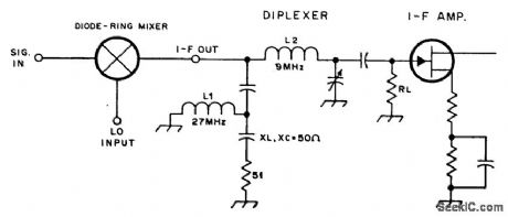
By inserting a high-pass filter section in the IF lead, this mixer is terminated at all frequencies, besides the IF, for other mixer products, which results in improved IMD. In this example, high-pass filter section L1 and capacitors cut off below 28 MHz. Above this frequency, the mixer is terminated.
(View)
View full Circuit Diagram | Comments | Reading(929)
1_Hz_TO_30_VOLTAGE_TO_FREQUENCY_CONVERTER
Published:2009/7/9 4:59:00 Author:May
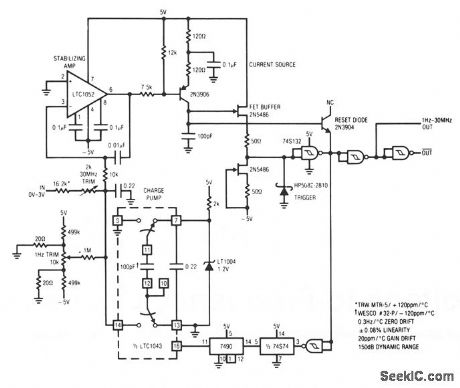
Circuit has a 1 Hz-to-30 MHz output, 150-dB dynamic range, for a 0 to 5 V input. It maintains 0.08% linearity over its entire 7 1/3 decade range with a full-scale drift of about 20 ppm/°C. To get the additional bandwidth, the fast JFET buffer drives the Schottky TTL Schmitt trigger. The Schottky diode prevents the Schmitt trigger from ever seeing negative voltage at its input. The Schmitt's input voltage hysteresis provides the limits which the oscillator runs between. The 30-MHz, full-scale output is much faster than the LTC1043 can accept, so the digital divider stages are used to reduce the feedback frequency signal by a factor of 20. The remaining Schmitt sections furnish complementary outputs. (View)
View full Circuit Diagram | Comments | Reading(713)
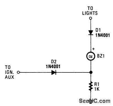
LIGHTS_ON_WARNING
Published:2009/7/9 4:57:00 Author:May
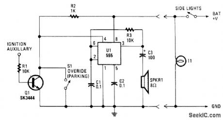
Because power for the circuit is obtained from the car's side lights, the circuit can't oscillate unless the lights are on. The reset pin on the 555 connects to transistor Q1. The base of Q1 is connected through R1 to the ignition auxiliary terminal on the car's fuse box. When the ignition is turned on, power is sup-plied to the base of Q1, which turns it on. With Q1 turned on, pin 4 of U1 is tied low, which disables the oscillator and inhibits the alarm. If the ignition is tumed off while the lights are on, power is applied to the 555 and Q1 is turned off, and the alarm starts. Switch S1 is an optional override. (View)
View full Circuit Diagram | Comments | Reading(849)
SELF-OSCILLATING_FLYBACK-SWITCHING_CONVERTER
Published:2009/7/9 4:52:00 Author:May
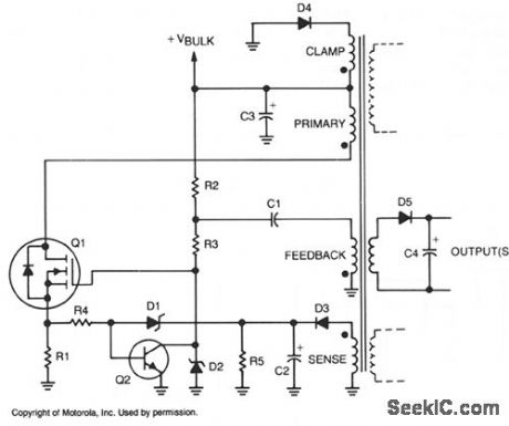
Regulation is provided by taking the rectified output of the sense winding and applying it as a bias to the base of Q2 via zener D1. The collector of Q2 then removes drive from the gate of Q1. Therefore, if the output voltage should increase, Q2 removes the drive to Q1 earlier, shortening the on time, and the output voltage will remain the same. Dc outputs are obtained by merely rectifying and filtering secondary windings, as done by D5 and C4. (View)
View full Circuit Diagram | Comments | Reading(1853)
REAR_FOG_LIGHT_CONTROLLER_WITH_DELAY
Published:2009/7/9 4:51:00 Author:May
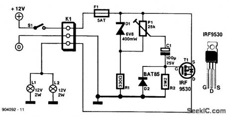
We assume that most of our readers are thoughtful drivers who do not switch on their rear fog lights when closely followed by other traffic. Following drivers (for an instant) will think that you are braking (although they have seen no reason for your doing so) and thus slam on their brakes as well. This could cause a very dangerous situation. Avoid a potentially dangerous action and install the rear fog light delay circuit, presented here.
Switch S1 is the on/off control for rear fog lights L1 and L2. As soon as this switch is closed, the gatesource voltage (Vgs) of MOSFET T1 will become more and more negative. Thus, the IC will conduct harder and harder. This in turn causes the brightness of the lights to gradually become brighter. Maximum brightness is reached after a delay of about 20 seconds, which is determined by time constant R2/C1.
The gate of T1 can be given a bias by preset Pl. This provides compensation for the initial period after the lights are switched on and the lamps do not light, because they need hundreds of milliamperes before they can do so. With Pl set correctly, the lamps will light, albeit weakly, and immediately the control switch is closed. The gate potential is then equal to the voltage at the wiper of Pl (remember that C1 is then still discharged).
Although the dissipation of T1 is a maximum during the transitional period (between switch on and the lamps lighting brightly), the heatsink required is calculated on the basis of the dissipation when the lamps light brightly. (View)
View full Circuit Diagram | Comments | Reading(877)
ELECTRONIC_DICE
Published:2009/7/9 4:51:00 Author:May
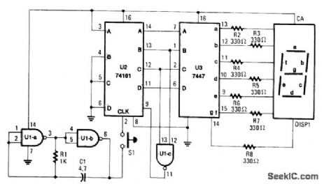
When S1 is pressed, counter U2 is driven by oscillator U1A/U1B and the count (0 through 6) is read on DISP1. R1 and C1 determine the count rate, which should be fast enough to ensure a random count. (View)
View full Circuit Diagram | Comments | Reading(0)
12_TO_16_V_CONVERTER
Published:2009/7/9 4:49:00 Author:May
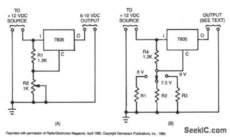

Many devices operate from a car's 12-V electrical system. Some require 12 V; others requtre some lesser voltage. An automobile battery's output can vary from 12 to 13.8 V under normal circumstances. The load requirements of the device might vary. This circuit maintains a constant voltage regardless of how those factors change. Simple circuit, A, uses a 7805 voltage regulator. In addition to a constant output, this IC provides overload and short-circuit protection. That unit is a 5-V, 1-A regulator, but when placed in circuit B, it can provide other voltages as well. When the arm of potentiometer R1 is moved toward ground, the output varies from 5 to about 10 V. (View)
View full Circuit Diagram | Comments | Reading(776)
DUAL_OUTPUT±12_OR±15_V_DC_DC_CONVERTER
Published:2009/7/9 4:44:00 Author:May
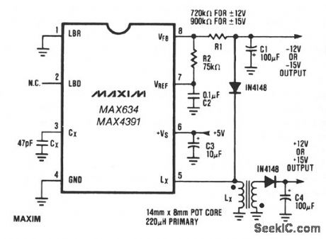
The buck-boost configuration of the MAX634 is well suited for dual output dc-dc converters Only a second winding on the inductor is needed. Typically, this second winding is bifilar-primary and secondary are wound simultaneously using two wires in parallel. The inductor core is usually a toroid or a pot core. The negative output voltage is fully regulated by the MAX634. The positive voltage is semiregulated, and will vary slightly with load changes on either the positive or negative outputs. (View)
View full Circuit Diagram | Comments | Reading(1351)
WHEEL_OF_FORTUNE
Published:2009/7/9 4:41:00 Author:May
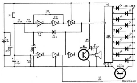
This circuit is a 10-LED spinning wheel that clicks as the wheel passes each point. The rotation starts fast, then gradually slows down to a random stop (with a click at each position). After the rotation ceases, the selected LED stays lit for about 10 seconds, then goes out. The cycle restarts by depressing (View)
View full Circuit Diagram | Comments | Reading(3190)
15_W_OFFLINE_CONVERTER
Published:2009/7/9 4:41:00 Author:May
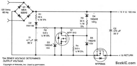
This nonisolated, unregulated, minimum component converter fills the void between low-power zener regulation and the higher power use of a 60-Hz input transformer. It is intended for use wherever a nonisolated supply can be used safely.The circuit operates by conducting only during the low-voltage portion of the rectified sine wave. R1 and D2 charge C1 to approximately 20 V, which is maintained by Q1. This voltage is applied to the gate of Q2, turning it on. When the rectified output voltage exceeds the zener voltage of D4, Q1 turns on, shunting the gate of Q2 to ground, turning it off. (View)
View full Circuit Diagram | Comments | Reading(704)
REGULATED_15_VSUBOUT_SUB_6_V_DRIVEN_CONVERTER
Published:2009/7/9 4:37:00 Author:May
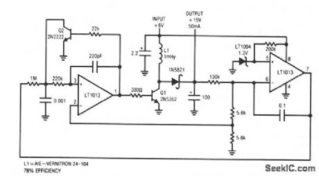
This converter delivers up to 50 mA from a 6-V battery with 78% efficiency. This flyback converter functions by feedback-controlling the frequency of inductive flyback events. The inductor's output, rectifted and filtered to dc, biases the feedback loop to establish a stable output. If the converter's output is below the loop setpoint, A2's inputs unbalance and current is fed through the 1-MΩ resistor at A1. This ramps the 1000-pF value positive. When this ramp exceeds the 0.5-V potential at A1's positive input, the amplifier switches high. Q2 turns on, discharging the capacitor to ground. Simultaneously, regenerative feedback through the 200-pF value causes a positive-going pulse at A1's positive input, sustaining Al's positive output. Q1 comes on, allowing inductor, L1, current to flow. When Al's feedback pulse decays, its output becomes low, turning off Q1. Q1's collector is pulled high by the inductor's flyback and the energy is stored in the 100-μF capacitor. The capacitor's voltage, which is the circuit output, is sampled by A2 to close a loop around A1/Q1. This loop forces A1 to oscillate at whatever frequency is required to maintain the 15-V output.In-phase transformer windings for the drain and gate of TMOS power FET Q1 cause the circuit to oscillate. Oscillation starts when the feedback coupling capacitor, C1, is charged from the supply line via a large resistance; R2 and R3 limit the collector current to Q2. During pump-up the on time is terminated by Q2, which senses the ramped source current of Q1. C1 is charged on alternate half-cycles by Q2 and forward-biased by zener D2.When the regulated level is reached, forward bias is applied to Q2, terminating the on time earlier at a lower peak current. When this occurs, the frequency increases in inverse proportion to current, but the energy per cycle decreases in proportion to current squared. Therefore, the total power coupled through the transformer to the secondary is decreased. (View)
View full Circuit Diagram | Comments | Reading(586)
| Pages:223/471 At 20221222223224225226227228229230231232233234235236237238239240Under 20 |
Circuit Categories
power supply circuit
Amplifier Circuit
Basic Circuit
LED and Light Circuit
Sensor Circuit
Signal Processing
Electrical Equipment Circuit
Control Circuit
Remote Control Circuit
A/D-D/A Converter Circuit
Audio Circuit
Measuring and Test Circuit
Communication Circuit
Computer-Related Circuit
555 Circuit
Automotive Circuit
Repairing Circuit