
Index 233
_SPEED_CONTEOLLED_REVERSIBLE_DC_MOTOR_VRIVE
Published:2009/7/8 5:12:00 Author:May
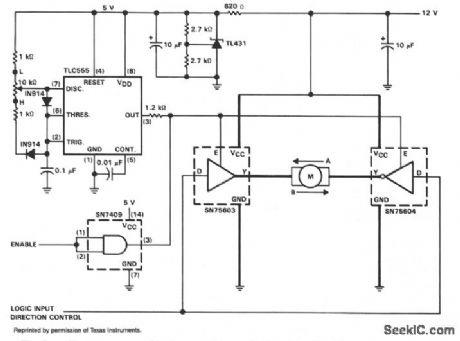
The figure illustrates a reversible dc motor drive application with adjustable speed control. The D inputs for these drivers are complementary and can be tied together and driven from the same logic control for bidirectional motor drive. The enables are tied together and driven by a pulse-width-modulated generator providing on duty cycles of 10 to 90% for speed control. A separate enable control is provided through an SN7409 logic gate. See the truth table for this motor controller application.
Definitions for the terms used in the truth table are as follows:
EN EnableDC Direction controlSP.C Speed controlA Direction of current-right to leftB Direction of current-left to rightH Logic 1 voltage levelL Logic 0 voltage levelN Speed control set for narrow pulse width Speed control set for wide pulse widthX Irrelevant (View)
View full Circuit Diagram | Comments | Reading(2085)
300_W_LINEAR_SOLID_STATE
Published:2009/7/8 5:08:00 Author:May
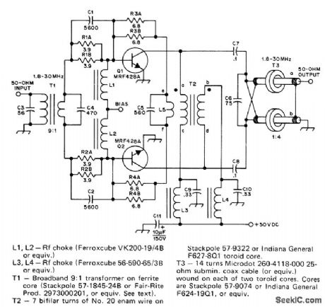


Class A circuit using two MRF428A transistors is emitter-bal-lasted to ensure even current-sharing. Requires separate 0.5-1V regulated bias voltage source, circuit for which is given in article along with design procedure for amplifier. Second part of article (May 1976, p 28-30) tells how to combine four 300-W amplifiers to get 1-kW output for 1.8-30 MHz.-H. O. Granberg, One KW—Solid-State Style, QST, April 1976, p 11-14. (View)
View full Circuit Diagram | Comments | Reading(786)
5_DIGIT_THERM_OM_ETER
Published:2009/7/8 4:56:00 Author:May
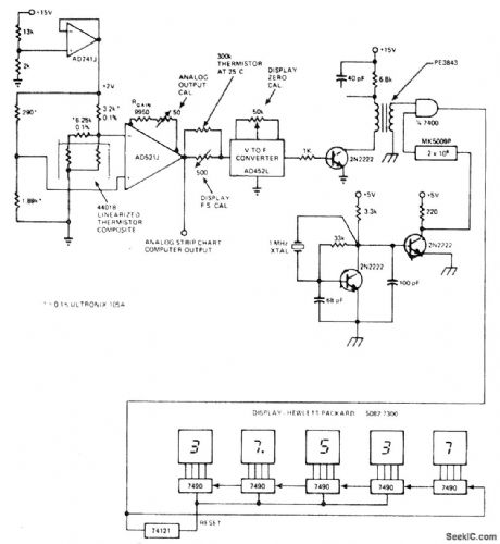
Temperature-to-frequency converter drives digital display providing0 .001°C resolution with 0.15°C absolute accuracy, Linearized thermistor network biases inverting input of AD521J instrumentation amplifier, while noninverting input is driven from same reference. Output can be fed directly to analog strip-chart recorder or computer, in addition to providing 0-10 V feed (for 0-100°C) to voltage-to-frequency circuit that drives display.Readout is updated at 2-s intervals.-J. Wil-Iiams, Designer's Guide to: Temperature Measurement, EDN Magazine, May 20, 1977, p 71-77.
(View)
View full Circuit Diagram | Comments | Reading(734)
FM_AUTO_RADIO_IF
Published:2009/7/8 4:52:00 Author:May
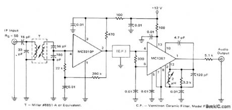
Uses MC1357 quadrature detector after ceramic filter to give IF bandwidth required for good stereo reproduction.Sensitivityis 18 μV for 3% total harmonic distortion.-''Integrated Circuit IF Amplifiers forAM/FM and FM Radios,'' Motorola,Phoenix,AZ,1975,AN-543A,p 6. (View)
View full Circuit Diagram | Comments | Reading(1745)
THERMISTOR_THERMOMETER
Published:2009/7/8 4:51:00 Author:May
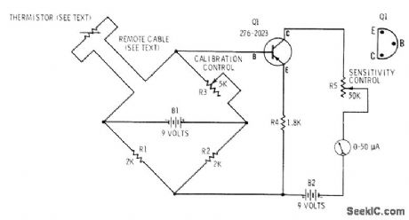
Thermistor for desired temperature range is one leg of Wheatstone bridge driving microammeter through transistor to provide direct indication of temperature. Can also be used for control purposes if suitable amplifier and relay are used in place of meter. Thermistor cable can be or-dinary parallel or twisted wires. To calibrate, immerse thermistor in water at various tem-peratures and measure water temperature with conventional high-accuracy thermometer. Cal-ibration graph can then be prepared as guidefor marking meter scale.-F. M. Mims, Transistor Projects, Vol. 1, Radio Shack, Fort Worth, TX, 1977, 2nd Ed., p 86-93. (View)
View full Circuit Diagram | Comments | Reading(3328)
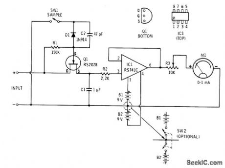
SAMPLE_READOUT_AMPLIFIER
Published:2009/7/20 21:13:00 Author:Jessie
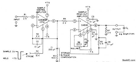
RCA CA3080A oporational trans conductance amplifier feeds CA3130 to give amplification of sampled signal. Input voltage is sampled for duration of strobe pulse and held for readout.- Linear Integrated Circuits and MOS/FET's, RCA Solid State Division,Somerville,NJ,1977,P165-170. (View)
View full Circuit Diagram | Comments | Reading(779)
TWO_SLEW_RATES
Published:2009/7/20 21:11:00 Author:Jessie
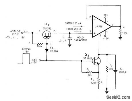
Cost of sample-and-hold circuits is reduced by using high slew rate only during sample period. Programmable μA776 opamp permits switching from high rate requiring 50-nA input bias current to holding amplifier mode requiring only 750-pA input bias current. Output level is held constant within 1% for about 2 s, making circuit ideal for digital readouts.-M. K. Vander Kooi, Low Cost Sample-and-Hold Circuit, EDN/EEE Magazine, Nov.1,1971, p 46. (View)
View full Circuit Diagram | Comments | Reading(1374)
256_8_BIT_SAMPLE_STORE
Published:2009/7/20 21:18:00 Author:Jessie
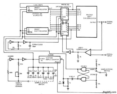
Low-cost substitute for storage oscilloscope can be used to study analog variables in speech synthesis, transient signal analysis, and destructive testing of components. Circuit is basically a tracking A/D convener whose digital output is fed into shift register holding 256 8-bit words. Separate clock for shift register is continuously adjustable from about 250 kHz down to about 4 s per cycle, with output going to 12-stage ripple counter. At 250 kHz, shift register stores input signal for t ms. Article gives details of circuit operation.-K. P. Roby, Transient Signal Analyzer Has Multiple Uses, EDN Magazine, Oct. 20,1974,p 46-48. (View)
View full Circuit Diagram | Comments | Reading(1258)
TRACK_AND_HOLD
Published:2009/7/20 21:15:00 Author:Jessie
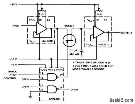
When track input control is 0.8V or less, gate in SN75180 holds 2N4391 transistor source-drain path closed so input signal goes to output unchanged. When control voltage is increased to 2 V, gate opens path through transistor, so signal voltage stored at that instant in 0.1-μF capacitor is held at output. Track time is greater than 500 ns for 1.V input, giving hold time over 6 s. Circuit uses two SN72310 wideband voltage-follower opamps.- The Linear and Interface Circuits Data Book for Design Engineers, Texas Instruments, Dallas, TX, 1973, p 4-41. (View)
View full Circuit Diagram | Comments | Reading(0)
16_digit_multiplex_circuitry_for_LED
Published:2009/7/20 22:16:00 Author:Jessie
16-digit multiplex circuitry for LED (courtesy Motorola Semiconductor Products Inc.). (View)
View full Circuit Diagram | Comments | Reading(834)
8_digit_multiplexed_LED
Published:2009/7/20 22:12:00 Author:Jessie
8-digit multiplexed LED (courtesy Motorola Semiconductor Products Inc.). (View)
View full Circuit Diagram | Comments | Reading(1402)
FET_OPAMP_SAMPLE_AND_HOLD
Published:2009/7/20 21:40:00 Author:Jessie
Meter indicates output signal when input is present and stores input in C1 when samples witch is open. Opamp is connected as unity-gain voltage follower. Charge on C1 will be drained within a few minutes by opamp shown. Charge can be held longer by changing to FET-input opamp or by opening both battery circuits with alternative DPDT switch SW2.Developed for classroom demonstrations.-F. M. Mims, Integrated Circuit Projects, Vol. 4, Radio Shack, Fort Worth, TX, 1977, 2nd Ed., p 61-69. (View)
View full Circuit Diagram | Comments | Reading(776)
15_V_SINGLE_SUPPLY
Published:2009/7/20 21:37:00 Author:Jessie
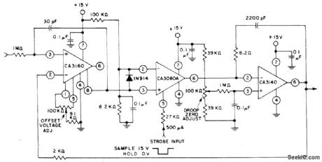
CA3160 opamp provides high input impedance and input voltage range of 0-10V. CA3080A functions as strobed current source for CA3140 output integrator and storage capacitor. Pulse droop during hold interval can be reduced to zero by adjusting 100K pot.- Linear Integrated Circuits and MOS/FET's, RCA Solid State Division, Somerville, NJ, 1977, p 271-272. (View)
View full Circuit Diagram | Comments | Reading(1554)
SAMPLE_AND_HOLD
Published:2009/7/20 21:36:00 Author:Jessie
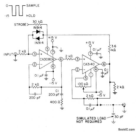
CA3140 bipolar M0S opamp serves as readout amplifier for storage capacitor C1 which is charged by CA3080A variable opamp serving as input buffer and low-feedthrough transmission switch. CA3140 also provides offset nulling.- Circuit Ideas for RCA Linear ICs, RCA Solid State Division, Somerville, NJ, 1977, p 17. (View)
View full Circuit Diagram | Comments | Reading(0)
TRACK_AND_HOLD_UP_TO_4_kHz
Published:2009/7/20 21:35:00 Author:Jessie
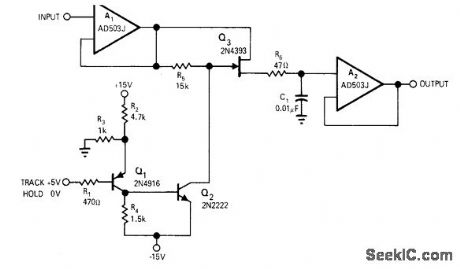
Developed for tracking ±10 V AF input signal when control input is +5 V. When control drops to 0 V, series FETQ3 opens and input voltage at that time is stored on C1 for transfer to output through high impedance opamp A2.-R. S. Burwen, Track-and-Hold Amplifier, EDNIEEE Magazine, Sept.1, 1971, p 43. (View)
View full Circuit Diagram | Comments | Reading(781)
NEUTRALIZATION_OVER_±75V_RANGE
Published:2009/7/20 21:27:00 Author:Jessie
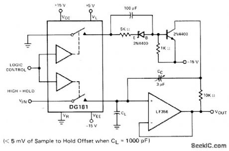
Switching transients are attenuated in sample-and-hold circuit using DG181 FET analog switch by adding neutralization derived from complementary signal coupled through upper switch of DG181. Charge transferred from second switch is then opposed to that from main channel. Circuit is controlled by input logic signal. With compensation, change in transferred charge is less than 5 picocoulombs for input signal range from -7.5 V to +7.5 V.- Analog Switches and Their Applications, Siliconix, Santa Clara, CA, 1976, p 7-61. (View)
View full Circuit Diagram | Comments | Reading(623)
ANALOG_SAMPLE_AND_HOLD
Published:2009/7/20 21:25:00 Author:Jessie
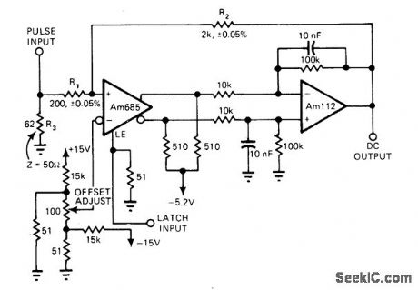
Uses AM685 comparator for continuous sampling of analog voltage at summing node formed by R1, and R2.Complementary logic outputs of comparator drive differential indicator formed by AM112 opamp. When error voltage at summing node is positive, comparator latches in high state and causes output opamp to integrate toward more negative voltage. When error voltage at latch time (determined by pulse input) is negative, integrator voltage ramps to more positive value. Circuit soon reaches equilibrium, at which out-put voltage is equal to -10 times value of sampled waveform. Article gives performance waveforms for sampling video pulses.-S. Den-'clinger, High-Speed Analog Sampler Uses Only Two IC's, EDN Magazine, May 20, 1977, p 128 and 130. (View)
View full Circuit Diagram | Comments | Reading(1040)
DIGITAL_SAMPLE_AND_HOLD
Published:2009/7/20 21:22:00 Author:Jessie
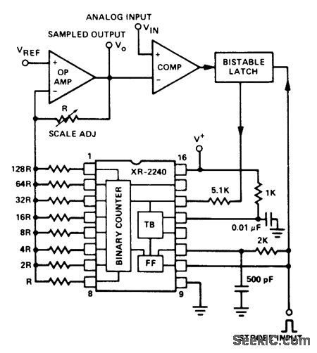
When strobe input is applied, RC low-pass network between reset and trigger inputs of Exar XR-2240 programmable timer/counter resets and then triggers timer, sets output of bistable latch to high state, and activates counter. Circuit generates staircase voltage at opamp output. When stair-case level reaches that of analog input to be sampled, comparator changes state, activates bistable latch, and stops count. Opamp output voltage level then corresponds to sampled analog input. Sample is held until next strobe signal. Minimum recycle time is about 6 ms. Sup-ply voltage can be 4-15V.- Timer Data Book, Exar Integrated Systems, Sunnyvale, CA, 1978, p11-18. (View)
View full Circuit Diagram | Comments | Reading(873)
5_digit_LED
Published:2009/7/20 21:56:00 Author:Jessie
5-digit LED (courtesy Motorola Semiconductor Products Inc.). (View)
View full Circuit Diagram | Comments | Reading(716)
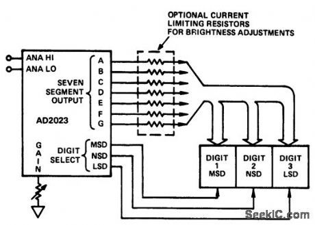
3_digit_ISUP2_SUPL_DPM_with_LED_interface
Published:2009/7/20 21:55:00 Author:Jessie
3-digit I2L DPM with LED interface (courtesy Analog Devices, Inc.). (View)
View full Circuit Diagram | Comments | Reading(536)
| Pages:233/471 At 20221222223224225226227228229230231232233234235236237238239240Under 20 |
Circuit Categories
power supply circuit
Amplifier Circuit
Basic Circuit
LED and Light Circuit
Sensor Circuit
Signal Processing
Electrical Equipment Circuit
Control Circuit
Remote Control Circuit
A/D-D/A Converter Circuit
Audio Circuit
Measuring and Test Circuit
Communication Circuit
Computer-Related Circuit
555 Circuit
Automotive Circuit
Repairing Circuit