
Index 235
0_100°F_GIVES_0_1_kHz_OUTPUT
Published:2009/7/8 5:04:00 Author:May
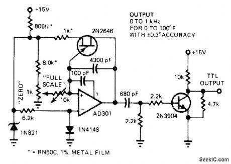
Circuit provides direct temperature-to-frequ ency conver-sion at low cost for applications where digital output is desked. Temperature sensor is 1N4148 diode having -2.2 mV/°C temperature shift, controlling AD301 opamp in relaxation oscillator drcuit. Compensated 1N821 zener stabilizes against supply changes. Output network using 680 pF and 2.2K differentiates 400-ns reset edge of negative-going output ramp of opamp and drives single-transistor inverter to provide TTL output. Accuracy is within 0.3°F.-J. Williams, Designer's Guide to: Temperature Measurement, EDN Magazine, May 20, 1977, p 71-77.
(View)
View full Circuit Diagram | Comments | Reading(1524)
FOUR_THERMOCOUPLE_MULTIPLEXING
Published:2009/7/8 5:00:00 Author:May
Low power dissipation in DG306 analog switches means lower offset voltages added to thermo-couple voltages by silicon in contact with aluminum in switches. Thermocouples are switched differentially to instrumentation amplifier driving meter, in order to cancel thermal offsets due to switch.- Analog Switches and Their Applications, Siliconix, Santa Clara, CA, 1976, p 7-87. (View)
View full Circuit Diagram | Comments | Reading(567)
_125_to__200℃_WITH_1°_ACCURACY
Published:2009/7/8 4:50:00 Author:May
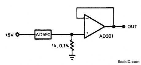
Use of factory-trimmed AD590 IC temperature sensor gives wide temperature range with minimum number of parts. Other temperature scales can be obtained by offsetting AD301 buffer opamp.-J. Williams, Designer's Guide to: Temperature Measurement, EDN Magazine, May 20, 1977, p 71-77. (View)
View full Circuit Diagram | Comments | Reading(989)
PWM_SPEED_CONTROLAND_ENERGY_RECOVERING_BRAKE
Published:2009/7/8 4:48:00 Author:May
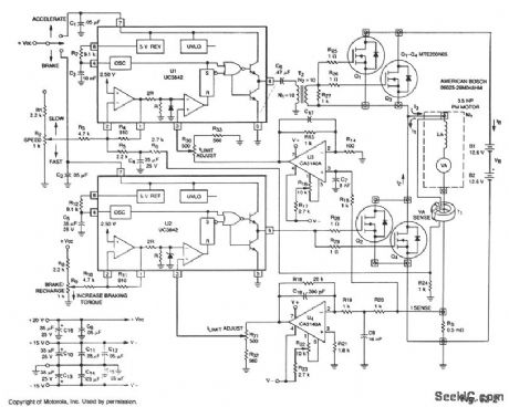
This circuit uses the main drive motor as a generator/brake to recover the battery charge during vehicle braking. When this is done, it can increase the overall range and efficiency of an electric vehicle.
In the accelerate mode, Q1 through Q3 receive gate pulses from U1, an on-line, current-mode, PWM controller IC. Assuming negligible effects of R, when Q1 through Q3 turn on, current I1 builds up through the motor at a rate of:
d/I1=VB-VA
where: VA = Battery voltage VB= Motor's back EMF LA = Motor inductance in henries
Motor current and torque continue to rise until the voltage on the ISENSE line is greater than IRESET, as determined by the speed potentiometer. At this time, Q1 through Q3 are switched off, current I2 begins to flow and decreases at a rate of: dI2 VA — = — dt LA
until the next clock period begins.As vehicle braking occurs, accelerate PWM IC U1 is switched off and braking PWM IC U2 and Q2 through Q4 are switched on. During this time, the back EMF source voltage causes current I3 to begin to flow at the rate of:
dI3 VA — = — dt LA
The current I3 continues to rise until ISENSE is greater than IRESET. Now, Q2 through Q4 are switched off and IB is forced to flow back into the storage battery, thus energy is recovered.
The braking torque produced by the motor is proportional to the average reverse current that flows through the motor on the duty cycle of Q2 through Q4. The braking force can continue until: VA =0
For reliable performance, voltage supplies should be independent of the main battery voltage.
(View)
View full Circuit Diagram | Comments | Reading(1300)
70_80°C_THERMOMETER
Published:2009/7/8 4:44:00 Author:May
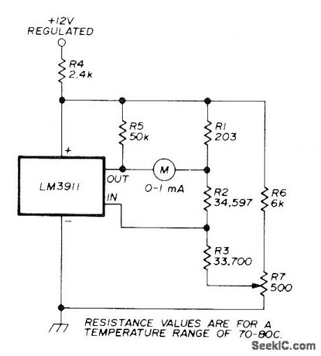
Uses National LM3911 IC having built-in temperature sensor.If no thermometer is available for calibration, set pot R7 to its midpoint. Article gives equations for calculating resistance values for other temperature and meter ranges. Applications indude monitoring of temperature in crystal oven. If permanenUy connected meter is not required, terminals can be provided for checking temperature with multimeter.-F. Schmidt, Precision Temperature Control for Crystal Ovens, Ham Radio, Feb. 1978, p 34-37. (View)
View full Circuit Diagram | Comments | Reading(583)
135_kHz_STRIP
Published:2009/7/8 4:41:00 Author:May
Developed for use in all-band VHF/UHF/S-band receiver. Operates from 12-Vsupply, connected to positive terminal of C11 through 100-ohm resistor.Articlee covers design and construction.-B. Hoisington,Building a 135 kHz 1-F Strip,73 Magazine,Sept 1975,p127-130 and 132. (View)
View full Circuit Diagram | Comments | Reading(1190)
DOUBLE_SIDEBAND_SUPPRESSED_CARRIER_MODULATOR
Published:2009/7/8 4:41:00 Author:May
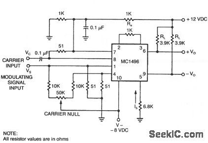
The basic current allows no carrier to be present in the output. By adding offsets to the carrier differential pairs, controlled amounts of carrier appear at the output. The amplitude becomes a function of the modulation signal-AM modulation.
(View)
View full Circuit Diagram | Comments | Reading(2038)
EQUALIZED_PREAMP_FOR_MAGNETIC_PHONOGRAPH_CARTRIDGES
Published:2009/7/8 4:41:00 Author:May
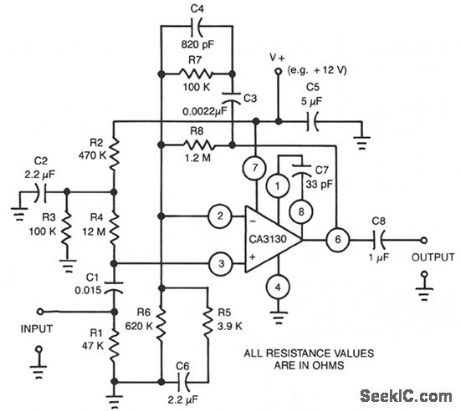
This circuit uses a CA3130 BiMOS op amp. Amplifier is equalized to RIAA playback frequency-response specif[cations. The circuit is useful as preamplifier following a magnetic tapehead. (View)
View full Circuit Diagram | Comments | Reading(1262)
BALANCED_MODULATOR
Published:2009/7/8 4:39:00 Author:May
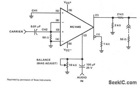
When the carrier level is adequate to switch the cross-coupled pair of differential amplifiers, the modulation signal, which has been applied to the gate, will be switched at the carrier rate, between the collector loads. When switching occurs, it will result in the modulation being multiplied by a symmetrical switching function. If the modulation gate remains in the linear region, only the first harmonic will be present. To balance the MC1445 modulator, equal gain must be achieved in the two separate channels. To remain in the linear region, the modulation input must be restricted to approximately 200 mV pk-pk. Because the gate bias point is sensitive to the amount of carrier suppression, a high-resolution, 10-turn potentiometer should be used. (View)
View full Circuit Diagram | Comments | Reading(0)
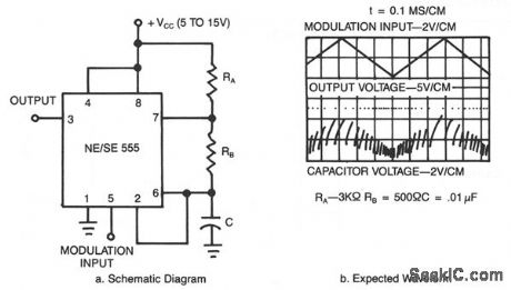
PULSE_WIDTH_MODULATOR
Published:2009/7/8 4:39:00 Author:May
In this application, the timer is connected in the monostable mode. The circuit is triggered with a continuous pulse train and the threshold voltage is modulated by the signal applied to the control voltage terminal at pin 5. This has the effect of modulating the pulse width as the control voltage varies. The figure shows the actual waveform generated with this circuit. (View)
View full Circuit Diagram | Comments | Reading(4060)
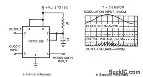
PULSE_POSITION_MODULATOR
Published:2009/7/8 4:38:00 Author:May
This application uses the timer connected for astable (free-running) operation, with a modulating signal again applied to the control voltage terminal. The pulse position varies with the modulating signal, since the threshold voltage and the time delay is varied. (View)
View full Circuit Diagram | Comments | Reading(1462)
BF_MODULATOR
Published:2009/7/8 4:36:00 Author:May
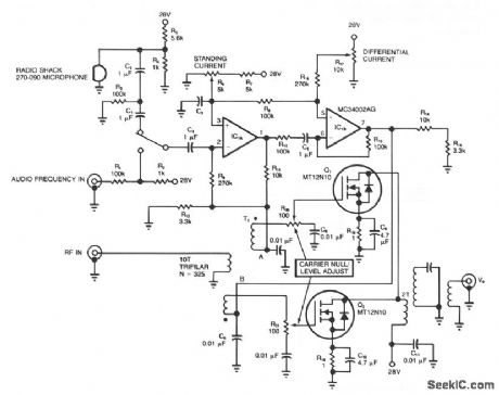
Because power MOSFETs offer high power gain at both audio and radio frequencies, they are useful in many areas of radio-circuit design. For rf applications, a MOSFET's large safe operating area, VDS vs ID, protects it against damage from reflected rf energy. As a modulator, a MOSFET's transfer linearity aids fidelity. In the suppressed-carrier modulator, an rf signal is applied to the primary of transformer T1, whose secondaries provide equal-amplitude, opposite-phase rf drive signals to output FETs Q1 and Q2.Output V0 is zero when no audio-frequency signals are present, because the opposite-phase rf signals from Q1 and Q2 cancel. When audio-frequency signals appear at nodes A and B, you obtain a modulated rf output (V0). Source resistors R18 and R19 improve the dc stability and low-frequency gain. A phase inverter, based on the dual op amp IC1A and IC1B, generates the out-of-phase, equal-amplitude, audio-frequency modulation signals. (View)
View full Circuit Diagram | Comments | Reading(831)
QMULTIPLIER_
Published:2009/7/8 4:34:00 Author:May

Transistorized Q multiplier can be connected to plate of mixer in receiver having IF in range of 1400-1500 kHz. Iron-core coil should have high a. Setting of pot depends on transistor used, which could also be HE-3 or 2N1742.-Q&A, 73 Magazine, April 1977,p 165. (View)
View full Circuit Diagram | Comments | Reading(1214)
SAW_SOCILLATOR_MODULATOR
Published:2009/7/8 4:34:00 Author:May
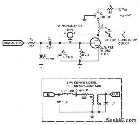
Adding a diode, a resistor, and a capacitor to the SAW (surface-acoustic-wave) oscillator allows you to use the oscillator in FSK (frequency-shift-keying) applications. D1, R1, and C1 form a simple diode switch in which D1 shunts C1 to ground. When the digital FSK input to R1 is low, D1 is off, and the small junction capacitance of D1 couples C1 to ground. A high FSK signal causes current to flow through R1 and D1.D1's dynamic impedance is small when it is in forward conduction. Therefore, C1 sees a lower impedance path to ground. Thus, the FSK input effectively switches C1 in and out of the oscillator's circuit.
When C1 is in the circuit-digital FSK is high-it pulls the frequency of the circuit slightly lower because of the additional phase shift C1 introduces at the GaGs FET gate terminal (available from: Dexcel, Div. of Gould, Santa Clara, CA). The SAW device (available from: RF Monolithics, Dallas, TX) restricts the amount of frequency shifting-usually less than 20 ppm for a high-Q SAW device.
The oscillator shown produces a center frequency of 896.2 MHz with an FSK deviation of 17 kHz when you drive the FSK input with a 0 to 5 V signal. The frequency also depends on L1 and C2.
(View)
View full Circuit Diagram | Comments | Reading(675)
SIGNAL_TRACK_AND_HOLD
Published:2009/7/8 4:34:00 Author:May
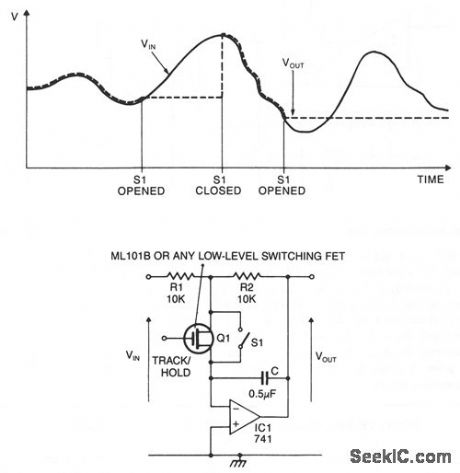
When the switch is closed or the FET is conducting, the circuit behaves as an inverting amplifier with a gain of R2/R1. Since as the inverting terminal of the op amp is a virtual ground, the capacitor is kept charged to the output voltage by the op amp. When the switch is opened and the FET is nonconducting, the voltage at the output is held constant by the capacitor, the current demands of the next stage are met by the op amp. The value of C should be chosen so that its impedance at the operating frequency is large compared to R1 and R2. (View)
View full Circuit Diagram | Comments | Reading(619)
107_MHz_IF_for_FM
Published:2009/7/8 4:32:00 Author:May
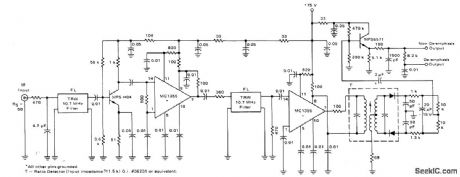
Motorola dual MC1355 limiting gain blocks are used with two TRW fivepole linear phase filters and external ratio detector to give complete high-performance IF amplifier for FM receiver. MPS-H04 discrete transistor is used after first filter block to reduce noise figure for overall system. Input and output impedances are 235 ohms.-''lntegrated Circuit IF Amplifiers for AM/FM and FM Radios, Motorola, Phoenix, AZ, 1975, AN-543A, p 4. (View)
View full Circuit Diagram | Comments | Reading(1475)
POSITIVE_AND_NEGATIVE_VOLTAGE_REFERENCE_TRACKER
Published:2009/7/8 4:31:00 Author:May

This reference uses an op amp to derive a negative output voltage that tracks with the positive reference voltage. A μA747 dual op amp, or any similar device such as an LM1458 or two pA741 devices, can be used.Positive Output = VD1×(R1+R2)/R2Negative Output =-Positive Output × R6/65 (View)
View full Circuit Diagram | Comments | Reading(1305)
RF_MODULATOR
Published:2009/7/8 4:31:00 Author:May
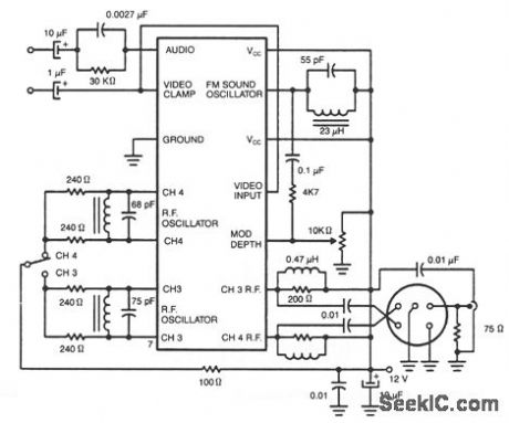
Two IC rf modulators convert a suitable baseband video and audio signal up to a low VHF modulated carrier-Channel 2 through 6 in the U.S., and 1 through 3 in Japan-the LM1889 and the LM2889. Both ICs are identical regarding the rf modulation function, including pin outs, and can provide either of two rf carriers with dc switch selection of the desired carrier frequency. The LM1889 includes a crystal-controlled chroma subcarrier oscillator and balanced modulator for encoding R through Y or U and V color difference signals. A sound intercarrier frequency lc oscillator is modulated using an external vatactor diode. The LM2889 replaces the chroma subcarrier function of the LM1889 with a video dc restoration clamp and an internal frequency-modulated sound intercarrier oscillator.
(View)
View full Circuit Diagram | Comments | Reading(5122)
SIGNAL_COMBINER
Published:2009/7/8 4:25:00 Author:May
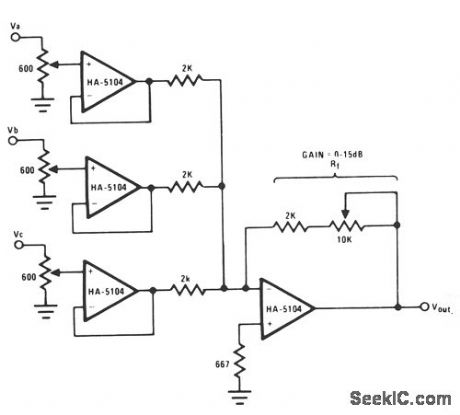
This circuit uses buffer stages to prevent channel crosstallk back through the mixer resistor network.The potentimeters used for each stage allow for convenient signal strength adjustment, while maintaining input impedance matching at the 600-Ω audio standard.The feedback resistor Rf will permit the output signal gain to be as high as 15 dB. (View)
View full Circuit Diagram | Comments | Reading(892)
DOOR_OPENER
Published:2009/7/8 4:24:00 Author:May
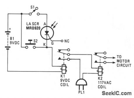
The door opener derives its power from a 9-V battery. A momentary-contact switch, S2, is provided in the event that manual opening and closing is required. Relay K1 is a 9-V type and relay K2 is a 117-Vac latching-type, which automatically latches with the first burst of current and opens on the second burst. The gate lead of the LASCR is not used;a light source triggers the LASCR unit into conduction, causing current to flow in the coil of the relay.That, in turn, causes K1's contacts to close,thereby energizing K2 (closing its contacts), and operating the garage door motor. (View)
View full Circuit Diagram | Comments | Reading(896)
| Pages:235/471 At 20221222223224225226227228229230231232233234235236237238239240Under 20 |
Circuit Categories
power supply circuit
Amplifier Circuit
Basic Circuit
LED and Light Circuit
Sensor Circuit
Signal Processing
Electrical Equipment Circuit
Control Circuit
Remote Control Circuit
A/D-D/A Converter Circuit
Audio Circuit
Measuring and Test Circuit
Communication Circuit
Computer-Related Circuit
555 Circuit
Automotive Circuit
Repairing Circuit