
Index 230
2__37_V
Published:2009/7/8 23:27:00 Author:May
Simple circuit glves fine linear controlwith 10-turn pot over wide voltage range by first using 10K trimmer pot to divide 7-V reference down to 2 V.-G. Dressel, Regulator Circuit Provides Linear 2-37 V Adjustment Range, EDNMagazine, March 5, 1978, p 122. (View)
View full Circuit Diagram | Comments | Reading(979)
TURNTABLE_RUMBLE_FILTER
Published:2009/7/8 23:27:00 Author:May
Many record players unfortunately exhibit two undesired side effects: rumble (noise caused by the motor and the turntable) and other low-frequency spurious signals. The active high-pass Chebyshev filter presented here was designed to suppress those noises. The filter has a 0.1-dB ripple characteristic and a cut-off point of 18 Hz.
The choice of a Chebyshev filter might not seem optimum for audio purposes, but because of its 0.1-dB ripple in the pass band it behaves very much like a Butterworth type. Its advantage is that the response has steeper skirts (which are calculated curves). Frequencies below 10 Hz are attenuated by more than 35 dB. The phase behavior in the pass band shows a gradual shift so that its effect on the repro-duced sound is inaudible.
If the filter is used in a stereo installation, the characteristics of both filters must be identical or nearly so. Phase differences between channels can be heard-perhaps not so much at lower frequencies, but certainly in the midranges. To ensure identity and also to obtain the desired characteristics, capacitors C1 through C5 must be selected carefully. It does not matter much whether their value is 467 or 473 pF; this difference only causes a slight shift of the cut-off point. However, they must be identical within that 1% tolerance. For symmetry of channels, the capacitors can be paired and then used in either channel at the corresponding position.
The diagram shows theoretical values for the resistors: their practical values are given in the table.The prototype was constructed with 5% metal-film types from the E12 series and these were used with-out sorting. Their tolerance was perfectly acceptable in practice.
The current drawn by the circuit is purely that through the op amp and it amounts to about 4 mA. The high cut-off point is also determined by the op amp and it lies at about 3 MHz.
The only problem that cannot be foreseen is a possible coupling capacitor in the signal source. That component will be in series with C1 and this might adversely affect the frequency response. However, if its value is greater than 47 μF, it will have little if any effect; if it is below that value, it is best removed; C1 will assume its function. (View)
View full Circuit Diagram | Comments | Reading(2783)
±15V_AT_200_mA
Published:2009/7/8 23:26:00 Author:May
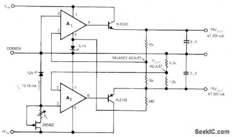
Two-opamp regulatorgives dual-polarity tracking outputs that can be balanced to within millivolts of each other or can be offset as required. Negative voltage is regulated, and positive output tracks negative. Article gives step-by-step design procedure based on use of pA741 or equivalent opamps. AC ripple is less than 2 mV P-P. Conventional full-wave bridge rectifier with capacitor-input filter can be used to provide rectuired unregulated 36 VDC for inputs.-C. Brogado, IC Op Amps Simplify Regulator Design, E.DNlEEEMagazine, Jan.15, 1972, p 30-34. (View)
View full Circuit Diagram | Comments | Reading(836)
1A_WITH_0005_VOLTAGE_ACCURACY
Published:2009/7/8 23:26:00 Author:May
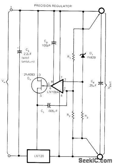
Use of National LM120 negative regulator with LM108A low-drift opamp and 1N829 precision reference diode gives extremely tight regula-tion, very low temperature drift, and full over load protection. Bridge arrangement sets output voltage and holds reference diode current constant. FET is required because 4-mA maximum ground current of regulator exceeds output current rating of opamp. R1 and R2 should track to 1 PPM or less. R3 is chosen to set reference current at 7.5 mA. For output of 8 to 14 V, use LM120-5.0; for 15-17V, use LM120-12.-C. T. Nelson, Power Distribution and Regulation Can Be Simple, Cheap and Rugged, EDNMagazine, Feb. 20, 1973, p 52-58. (View)
View full Circuit Diagram | Comments | Reading(842)
_3V
Published:2009/7/8 23:25:00 Author:May
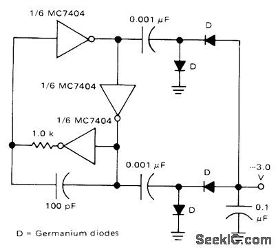
Circuit using three sections of Motorola MC7404 operates from +5 V supply and gen-erates -3 V at up to 100 μA, as one of supply voltages required by Motorola MCM6570 8192-bit character generator using 7 x 9 matrix.- A CRT Display System Using NMOS Memories, Motorola, Phoenix, AZ, 1975, AN.706A, p 5.|| (View)
View full Circuit Diagram | Comments | Reading(815)
_5V_WITH_MC146OG
Published:2009/7/8 23:24:00 Author:May
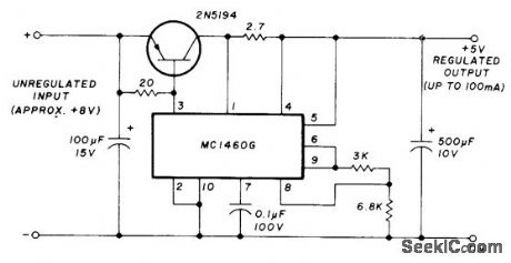
Series power transistor and Motorola IC voltage regulator provide up to 100 mA. IC shown has been replaced by MC1469. Equivalents made by other manufac-turers can also be used.-H. Olson, Power-Sup-ply Servicing, Ham Radio, Nov. 1976, p 44-50. (View)
View full Circuit Diagram | Comments | Reading(808)
LOOP_ANTENNA_FOR_35_MHz
Published:2009/7/8 23:22:00 Author:May

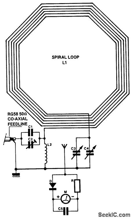

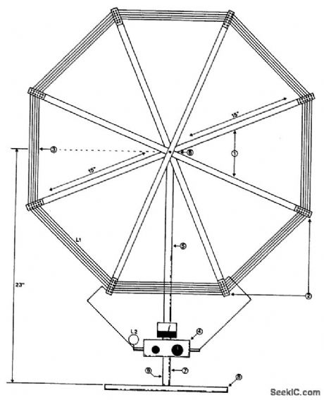
C1=3750 pF 500 V siver-mica capacitor.C2=100 pF preset capacitor(Jackson C803)C3=75 pF variable capacitor(Jackson C809),plus knob.C4=12.7 pF variable capacitor(Jackson C16),plus knob.C5=22 nF mica capacitor.M=250 μA f.s.d.40×40 mm moving coil meter(Maplin LB8O8).D=HF silicon diode.R=1 kΩ resistor(see text).L1=51/8 turns of PVC covered stranded 7/O.2 mm wlre,Outside diameter:1.2mm,1 kV/1.5 A rating(see text)L2=13 turns 16SWG tinned wlre,1 inch internal diameter.Feedline=48 inch RG58 coaxial cable,plus plug to suit transmitter.Box=ABS box type MB3,118×96×45 mm Maplin ref LH22.Terminal blocks=qty,412-way 2 amp terminal block Maplin ref,FE78.Spacers=qty.3 insulated spacer type M3,30 mm long,Mapin ref.FS4OT.Spokes=qty.48-foot lengths of 5/8×l/4inch molded hardwood(DIY store).Vertical support=23×O.8×0,Sinch wood(DIY store).Wood base=12×8×0.5 inch plywood or simiar.21/2 inch steel support bracket.
1. 4 lengths molded hardwood 3O x 5/8 x 1/4 Varnished. 2BA holes drilled in the centre. Glued and bolted together.2. 8 off 6-way 2-amp polythene terminal blocks used as insulated wire spacers.3. 51/8 turns of PVC stranded wire (for specs see component, list).4. See Fig. 3.5. Wood vertical support 23 x0.8 x0.8 , wood stained.6. 2 x 2BA bolt.7. Box front vertical support, 41/2 x 1/2 x 3/4 , wood stained.8. Wood base 12 x 8 x1/2 (for similar), wood stained.9. 21/2 steel support bracket behind wood vertical support.10. Drilled and secured with glue and c/s wood screws.Note: = inch=2.54cm.
Suitable for receiving or transmitting (10 W or less) on the 80-m band, this loop antenna might be helpful when an outside antenna is not possible. (View)
View full Circuit Diagram | Comments | Reading(1413)
RANGING_SYSTEM
Published:2009/7/8 23:19:00 Author:May
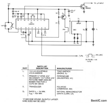
Combine an electrostatic transducer with an ultrasonic transceiver IC to build a ranging system that senses objects at distances from 4 inches to more than 30 feet. Transducer Y1's broadband characteristic simplifies tuning. The secondary of T1 resonates with the 500-pF capacitor C1 at a frequency between 50 and 60 kHz. You tune L1 to this frequency by using an oscilloscope to note the maximum echo sensitivity at pin 1. Step-up transformer T1 prov.ides 150-V bias for the transducer. (View)
View full Circuit Diagram | Comments | Reading(770)
SCRATCH_FILTER
Published:2009/7/9 1:34:00 Author:May
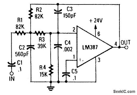
Designed to produce 12-dB/octave roll-off above the 10-kHz cutofffrequency, this LP active filter will help reduce needle scratch on records. It uses an LM387low-noise amplifier IC. (View)
View full Circuit Diagram | Comments | Reading(0)
SECOND_ORDER_100_Hz_HIGH_PASS_FILTER
Published:2009/7/9 1:32:00 Author:May
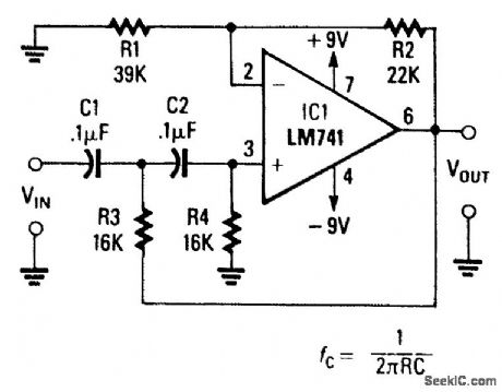
This second-order filter can be scaled change the cutoff frequencies. (View)
View full Circuit Diagram | Comments | Reading(912)
SIMPLE_RIPPLE_SUPPRESSOR
Published:2009/7/9 1:29:00 Author:May
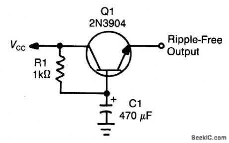


This circuit, at times called a capacitcance multiplier, is useful for suppression of power-supply rip-ple. C1 provides filtering that is equal to a capacitor of (B+1) C1, where B = dc current gain of Q1 (typi-cally > 50). (View)
View full Circuit Diagram | Comments | Reading(2055)
10_PPM_℃
Published:2009/7/8 23:17:00 Author:May
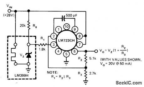
Connections shown convert LM723CH regulator into precision power reference having excellent long-term stability and temperature stability. LM399H replaces internal reference of LM723 with low-noise 6.9 V to give desired performance over temperature range from +15 to +65℃.-B. Welling, High-Stability Power Supply Uses 723 Regulator, EDNMaga-zine, Jan. 20, 1978, p 114 and 116. (View)
View full Circuit Diagram | Comments | Reading(3233)
TREMOLO_3
Published:2009/7/8 23:15:00 Author:May
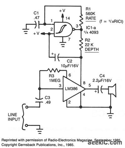
This simple circuit can color the sound cormng from your audio system. Clocking for the circuit is provided by an oscillator built from one quarter of a 4093 quad NAND Schmitt trigger. With the component values shown, it will run at about 5 Hz. The clock frequency is fed to the gain control, pin 8, of an LM386 amplifier. Tremolo is produced by varying the amplifier gain. A trimmer potentiometer can be put in series with R1, to easily experiment with different rates. To experiment, make R1 about 100-KΩ and use a 1-MΩ trimmer. That allows frequen-cies from about 2 to 20 Hz to pass. Resistor R2 is the depth control. It controls the degree of tremolo. To adjust, put a trimmer in series with R2. Make R2 a 5-KΩ unit and use a 50-KΩ trimmen Since the tremolo clock uses the gain-control pin of the amplifier, change the value of capacitor C4 in order to change the gain of the amplifter. Make C4 larger to increase the gain or smaller to decrease it. But. don't go any lower than 0.1 μF because you'll be cutting into the bottom-end frequency response. (View)
View full Circuit Diagram | Comments | Reading(927)
25_V_AT_10_A_FOR_LAB
Published:2009/7/8 23:14:00 Author:May
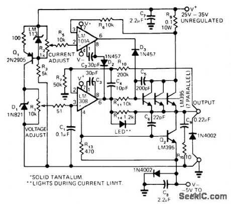
Circuit uses no large output capacitors yet has good response as constant-voltage or constant-current source.LM395 units (7 in parallel) act as current-limited thermally limited high-gain power transistor.Mount all on same heatsink for good current sharing, since 300 W will be dissipated under worst-case conditions. Only two control opamps are needed, oneforvoltage control and one for current control.-R. C. Dobkin, General-Purpose Power Supply Furnishes 10A and 25V, EDNMagazine, March 5, 1975, p 70. (View)
View full Circuit Diagram | Comments | Reading(698)
_15V_WITH_μA723
Published:2009/7/8 23:13:00 Author:May
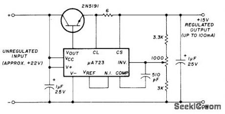
Series power transistor and Fairchild IC voltage regulator provide up to 100 mA. Article covers troubleshooting and repair of all types of regulators.-H. Olson, Power-Supply Servicing, Ham Fladio, Nov.1976, p 44-50. (View)
View full Circuit Diagram | Comments | Reading(749)
ELECTRONIC_TREMOLO
Published:2009/7/8 23:10:00 Author:May
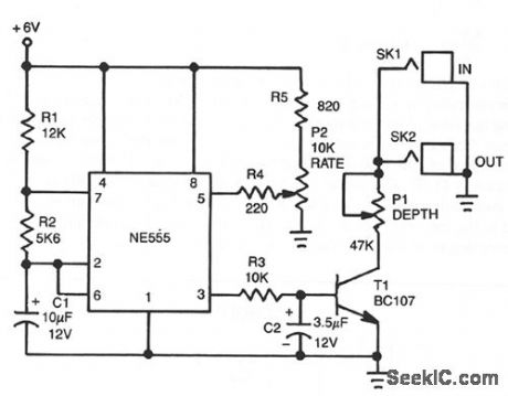
The tremolo effect is generated by a repeating volume change at a rate usually between 1 and 15 Hz. The timer produces a low frequency square wave that is smoothed by a simple rc integrator. This varying signal modulates the signal input from the instrument. Transistor T1 is used as a voltage controlled resistor. The output of the circuit is connected in parallel to the output of the instrument. Potentiometer P1 provides depth control by adjusting the amplitude of the modulating waveform applied to the instrument. The rate control frequency is set by potentiometer P2. (View)
View full Circuit Diagram | Comments | Reading(2435)
TREMOLO_1
Published:2009/7/8 23:07:00 Author:May
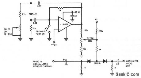
A phase shift oscillator using the LM324 operates at an adjustable rate, 5-10 Hz, set by the speed pot. A potion of the oscillator output is taken from the depth pot and used to modulate the on resistance of two 1N914 diodes operating as voltage controlled attenuators. Care must be taken to restrict the incoming signal level to less than 0.6 V pk-pk, or undesirable clipping will occur. (View)
View full Circuit Diagram | Comments | Reading(680)
0_20_Hz_DATA_DEMODULATOR
Published:2009/7/8 22:58:00 Author:May
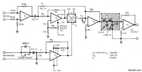
Used for measuring and monitoring suppressed-carriersignal modulation from alrcraft control sys-terms.Provides data frequency response,withhin o.1 dB from DC to 20 Hz,with linearity better than 0.1%. In-phase reference voltage applied to comparator IC5 controls gating of CD4016 MOS switch S1.Suppressed-carrier signal is buffered by opamp A1 for branching to summing junction of A3. Article describes operation of circuit.-J. A. Tabb and M. L. Roginsky, Instrumentation Signal Demodulator Uses LowPower IC's, EDN Magazine, Jan. 20, 1976, p 80. (View)
View full Circuit Diagram | Comments | Reading(674)
TUNABLE_AUDIO_FILTER
Published:2009/7/8 22:54:00 Author:May
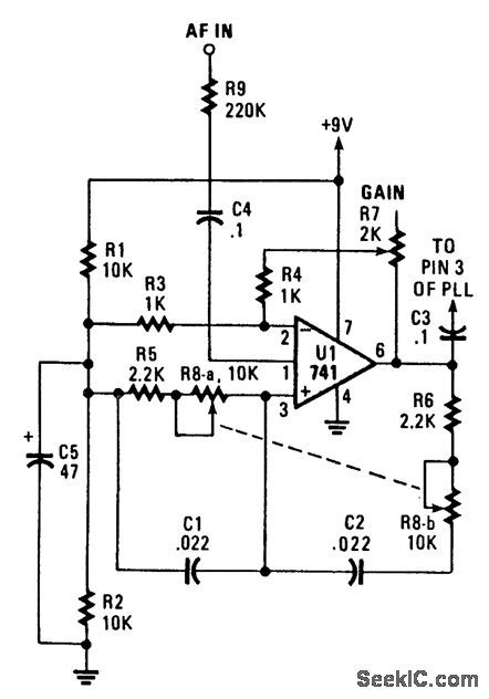
This circuit uses a Wien Bridge and variable negative feedback. R7 controls the gain and R8A and R8B controls the tuned frequency. (View)
View full Circuit Diagram | Comments | Reading(0)
DOOR_BUZZER
Published:2009/7/8 22:53:00 Author:May
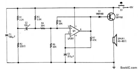
An LF357 functions as a swept-tone oscillator, driving Q1 and SPKRl. A 9-Vdc supply is required. (View)
View full Circuit Diagram | Comments | Reading(772)
| Pages:230/471 At 20221222223224225226227228229230231232233234235236237238239240Under 20 |
Circuit Categories
power supply circuit
Amplifier Circuit
Basic Circuit
LED and Light Circuit
Sensor Circuit
Signal Processing
Electrical Equipment Circuit
Control Circuit
Remote Control Circuit
A/D-D/A Converter Circuit
Audio Circuit
Measuring and Test Circuit
Communication Circuit
Computer-Related Circuit
555 Circuit
Automotive Circuit
Repairing Circuit