
Index 189
ULTRA_LONG_MONO_1
Published:2009/7/16 11:59:00 Author:Jessie
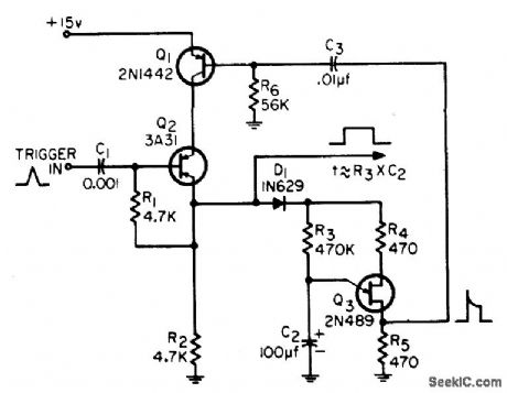
For applications having only light loading. If required to drive heavy loads, standby efficiency is reduced, and C3 must be so large that circuit could be acidentally turned off by negative supply bus transients.-J. C. Schaeffert and N. F. Goldman, Improved Ultra-Long Monostable Multivibrator, EEE, 12:12, p 57-58. (View)
View full Circuit Diagram | Comments | Reading(659)
HALF_WAVE_SYNCHRONOUS_RECTIFLER
Published:2009/7/12 23:51:00 Author:May
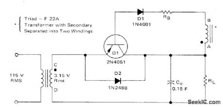
Transistoral is synchronously biased on by AC input voltage to give efficient low-voltage regulation. When points A and C are positive with respect to points B and D, base-emitter junction of Q1 is forward-biased and collector current flows through load RL. On negative alternations,Q1 is reverse-biased and transistor is blocked.-B. C. Shiner, Improving the Efficiency of Low Voltage, High-Current Rectification, Motorola, Phoenix, AZ, 1973, AN-517, p 3. (View)
View full Circuit Diagram | Comments | Reading(938)
DIGITAL_FREQUENCY_DOUBLER_CIRCUIT
Published:2009/7/12 23:51:00 Author:May
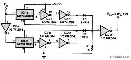
The 74LS393 is designed to advance one count on the positive-to-negative transition of the pulse at the clock input (pins 1 and 13). An inverter in front of the B section of the counter causes the B section to advance one count on the negative-to-positive transition of the input pulse. Each section of the counter is cleared with a positive-going pulse on the master reset input (pins 2 and 12). Positive-going output pulses from pins 6 and 10 of IC2 reset the respective counters. The duration of the pulses depends upon the propagation delay of the inverters. With the 74LS04 hex inverter, delay will probably be in the vicinity of 20 to 25 ns. The output pulses are also connected to the remaining inverter gate through switching diodes and a pull-down resistor, which configures the remaining inverter as a NOR gate. The output at pin 8 of IC2 represents the input frequency multiplied by 2. (View)
View full Circuit Diagram | Comments | Reading(2069)
2_5_min_STARTING_DELAY
Published:2009/7/12 23:50:00 Author:May
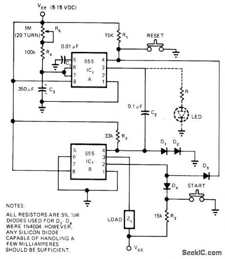
Energizing of load is delayed up to 5 min after start button is pushed, as required in some CMOS circuits and digital control systems. Uses pair of 555 timers, with A operating in straightforward timing mode and B connected as set-reset flip-flop. Pushing reset button initializes system, placing A in low state and making pin 3 of B high, leaving load unenergized. When start button is pushed, A goes high and begins timing out. After delay interval, output of B goes low, energizing load until system is reset. LED can be added to indicatethattiming is in progress.-J. C. Nichols, Versatile Delay-on-Energize Timer Uses Two 555's, EDN Magazine, Oct. 5, 1975, p 76and78. (View)
View full Circuit Diagram | Comments | Reading(959)
THERMISTOR_COMPENSATED_ONE_SHOT
Published:2009/7/16 11:58:00 Author:Jessie
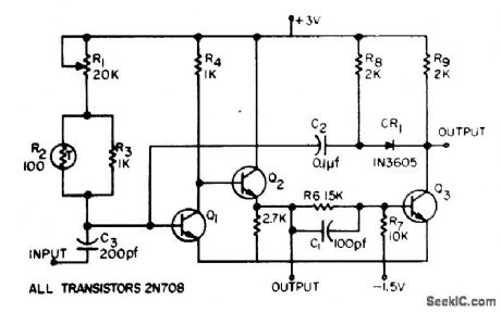
Negative-temperature-coefficient thermistor in pulse width determining network keeps pulse width of mvbr constant within 0.6% over range of 25℃. Basic period with values shown is 357 microsec, increasing to 359 microsec at temperature extremes.-B. Hedin, Temperature-Compensated One-Shot, EEE, 12:5, p 75. (View)
View full Circuit Diagram | Comments | Reading(688)
50_KC_FREE_RUNNING_MVBR
Published:2009/7/16 11:55:00 Author:Jessie
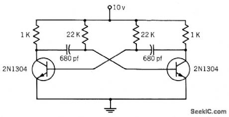
Uses 2N1304 transistors having base-emitter breakdown of -25 V, making emitter diodes unnecessary.-Texas Instruments Inc., Transistor Circuit Design, McGraw-Hill, N.Y., 1963, p 380. (View)
View full Circuit Diagram | Comments | Reading(748)
ADJUSTABLE_DUTY_CYCLE_MONO
Published:2009/7/16 11:54:00 Author:Jessie
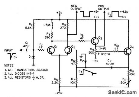
When ratio of pulse width to pulse spacing exceeds value set by R12, width of output pulse is automatically reduced to maintain duty cycle at preset maximum. Used as pulse driver for high-power amplifier when duty cycle must be limited to prevent overheating. If duty cycle is set for 50% and frequency is increased, output will be square wave for all frequencies up to maximum frequency limit for circuit. R9 adjusts output pulse width from 0.7 to 7 microsec.-D. N. Lee, Monostable Multi With Adjustable Duty Cycle, EEE, 13:9, p 92-94. (View)
View full Circuit Diagram | Comments | Reading(893)
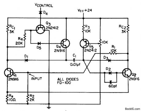
WIDE_RANGE_MONO
Published:2009/7/16 11:26:00 Author:Jessie
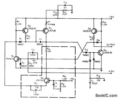
Adding one transistor(Q6)to linear one-shot increases frequency range 150 times.-G. Marosi, Wide Range Monostable Multivibrator, EEE, 13:9, p 76. (View)
View full Circuit Diagram | Comments | Reading(796)
FAST_RECOVERY_ONE_SHOT
Published:2009/7/16 10:49:00 Author:Jessie
Dynamic period can be varied linearly over range of 20 to 425 microsec. Retrigger time is only 3 microsec for short periods and 14 microsec for longest periods. Circuit is conventional except for d-c isolation diode D1 and drive resistor R4.-R. S. Hughes, A linear, Voltage-Variable One-Shot With Fast Retrigger Time, EEE, 13:5, p 78-79. (View)
View full Circuit Diagram | Comments | Reading(1105)
ORYSTAL_RADIO_COILS
Published:2009/7/12 23:45:00 Author:May
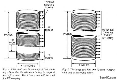
These coils are suitable for crystal sets and broadcast receiver experiments. They are wound with 19- or 20-gauge wire and should be wound on a material having low loss at AM broadcast frequencies. PVC or polystyrene tubing would be suitable, but cardboard or fiberglass will do as well. (View)
View full Circuit Diagram | Comments | Reading(998)
ANTENNA_MATCHED_CRYSTAL_RADIO
Published:2009/7/12 23:44:00 Author:May
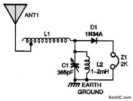
This receiver uses a tuning circuit that is, in some ways, similar to an antenna matching deviceused by amateur-radio operators to impedance-match their receiver/transmitter input/output Circuitry to the impedance of the antenna for maximum signal transfer, Inductor L2 provides a dc-signal return path for D1's output The inductance of L2 is too large to affect the circuit's tuning function. (View)
View full Circuit Diagram | Comments | Reading(1931)
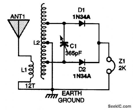
TUNABLE_DUAL_COIL_CRYSTAL_RADIO
Published:2009/7/12 23:43:00 Author:May
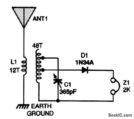
The 12-turn primary winding couples the RF signal from the antenna/ground system to the 48 turn secondary winding. Here C1, a 365-pF variable capacitor, tunes the L/C circuit to the desired radio-frequency signal. A 1N34A germanium diode, D1, detects the audio and feeds it to the headphones (Z1). The various taps on L1's secondary allow impedance matching of the antenna/ground system and the detector diode, as well as the inductance value needed to tune to the desired RF signal. (View)
View full Circuit Diagram | Comments | Reading(1961)
FULL_WAVE_DETECTOR_ORYSTAL_SET
Published:2009/7/12 23:42:00 Author:May
The 12-turn coil of L1 couples the RF signal to the large coil, L2. Connect the center tap of L2 to ground, the fourth tap up from the center to diode D1, and the fourth tap down from the center to diode D2. The combined audio output drives the headphones (Z1), If you change tap positions, keep the same number of turns on each side of center. That will balance the RF that feeds each detector diode. The circuit's sensitivity and audio output can be increased by placing L1 inside of L2 (the forms specified for the coils should make that possible). For maximum selectivity, L1 should be loose-coupled to L2. (View)
View full Circuit Diagram | Comments | Reading(1224)
SIMPLE_GUITAR_AMPLIFIER_WITH_DUAL_INPUTS
Published:2009/7/12 23:40:00 Author:May
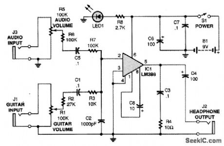
This amplifier uses an LM386 IC and has two inputs, an input for guitar and a separate audio input for a second guitar, a mike, etc. Power is supplied by a 9-V battery. While headphones are indicated, the amplifier will drive a small speaker. Output is around 300 to 500 mW, depending on load and battery voltage.
(View)
View full Circuit Diagram | Comments | Reading(4450)
130_AND_270_V_FOR_CRT
Published:2009/7/12 23:39:00 Author:May
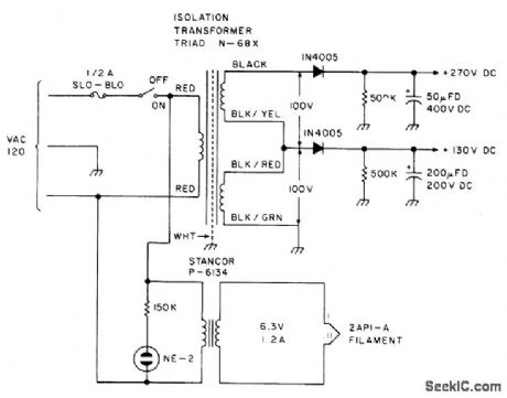
High-voltage power supply provides 270 V required for deflection plates of 2AP1-A CRT used as RTTY tuning indicator, as well as 130 V for high-voltage amplifier. Large capacitor keeps ripple voltage low.-R. R. Parry, RTfY CRT Tuning Indicator, 73 Magazine, Sept. 1977, p 118-120. (View)
View full Circuit Diagram | Comments | Reading(824)
12_V_EMERGENCY_POWER
Published:2009/7/12 23:35:00 Author:May
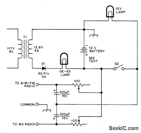
Trickle-charge circuit and 12-V motorcycle battery provide reliable emergency power for battery-operated weather radio, fiortable AM/FM receiver, or hand-held transceiver for many hours. 100K pots drop voltage to 9 V for each receiver. Lamp can be auto dome light. GE-63 pilot lamp in charging circuit acts as current limiter and charge indicator.-J. Rice, Simple Emergency Power, QST, March 1978, p 42. (View)
View full Circuit Diagram | Comments | Reading(1430)
TRACE_BRIGHTNESS_EQUALIZER
Published:2009/7/16 21:19:00 Author:Jessie
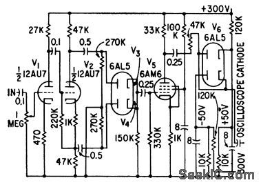
Amplitude of signal to be displayed controls scope brightness by changing voltage on cathode of crt. Low-level signal and high-voltage pulses are automaticallyadjusted as to brightness, so both traces appear equally bright on photographic film.-J. K.Goodwin, Circuit Evens Scope Brightness, Electronics, 31:51, p 96-98. (View)
View full Circuit Diagram | Comments | Reading(728)
0_10_min_WITH_1_s_ACCURACY
Published:2009/7/12 23:33:00 Author:May
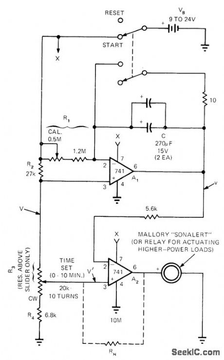
After calibration, accuracy is independent of battery voltage because source voltage affects charging voltage of C and threshold of comparator A2 equally. Time delay t fortimer is CR1R3/R2.-M. Strange, Simple Electronic Timer is Compact and Accurate, EDNMagazine, April20, 1973, p89 and 91. (View)
View full Circuit Diagram | Comments | Reading(767)
22_W_AMPLIFIER_FOR_12_V_SYSTEMS
Published:2009/7/12 23:28:00 Author:May
Power for the circuit (+12 V) is provided by a connection to the host vehicle's battery. A connection is also provided for the vehicle/s ground. Capacitors C1 and C2 provide decoupling of any sig-nal riding on the supply voltage, while capacitor C3, working in conjunction with IC1, provides ripple rejection. The incoming audio signal is coupled to IC1 by capacitors C4 and C5. Those 10-μF capacitors are used to avoid rolling off of the low audio frequencies. Resistor R1 and capacitor 06 feed the mute switch circuit (indluded in IC1), providing the delay that eliminates turn-on pop. Their R/C time constant is about 1.4 s. None of the component values external to IC1 are crucial, but major value substitutions should not be made. Pin 14 (the mute switch) of IC1 must have at least 8.5 V for the amplifier to be ON, or be held below 3.3 V to ensure that the chip stays in the mute condition. Current requirements at this pin are on the order of 40 pA in the ON condition, and 100 pA for standby. The R1/C6 combination used here (47μF and 39,000 Ω) provides enough delay to eliminate turn-on pop without having an excessive wait for normal operation. In addition to this slight delay, pin 14 gradually comes up above the 8.5-V threshold as C6 charges up, rather than coming on in-stantly, as it would if a simple switch were used. Values for C6 and RI are not crucial, but RI should be no larger than 100,000 Ω, and the R1/C6 time constant should be on the order of a second or two. Too short a time constant may not eliminate the turn-on pop; too long a time constant does not harm, except causing an irritating delay. (View)
View full Circuit Diagram | Comments | Reading(838)
12_VDC_TO_115_VAC_AT_400_Hz
Published:2009/7/12 23:27:00 Author:May
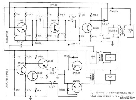
Provides threephase output at 20 W by using RC coupling to oscillator in such a way that 120°phase difference exists at collectors of 2N651 transistors of oscillator. Emitter-follower amplifier driving push-pull power output transistors is shown only for phase 1; other two phases use similar amplifiers, Power transistors are operated in saturated switching mode.-R. J. Haver, The ABC's of DC to AC Inverters, Motorola, Phoenix, AZ, 1976, AN-222, p 15. (View)
View full Circuit Diagram | Comments | Reading(1315)
| Pages:189/471 At 20181182183184185186187188189190191192193194195196197198199200Under 20 |
Circuit Categories
power supply circuit
Amplifier Circuit
Basic Circuit
LED and Light Circuit
Sensor Circuit
Signal Processing
Electrical Equipment Circuit
Control Circuit
Remote Control Circuit
A/D-D/A Converter Circuit
Audio Circuit
Measuring and Test Circuit
Communication Circuit
Computer-Related Circuit
555 Circuit
Automotive Circuit
Repairing Circuit