
Index 193
HIGH_FREQUENCY_LOOP_ANTENNA
Published:2009/7/12 22:10:00 Author:May
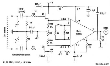
Good performance in the 5- to 30-MHz range requires an amplifier with extremely high input im-pedance and low noise that can drive 75-Ω loads at high signal levels at frequencies over 30 MHz.Combining dual FET source followers and the new Maxim 436 wideband transconductance amplifier can produce just such an amplifier. A balanced configuration is used for the tuned loop to preserve the symmetry of the figure-eight polar antenna pattern. As a result of using FET source followers on the amplifier's front end, only the 1-MΩ gate resistors load the tuned circuit, so tuning is very sharp and resistance to off-frequency interference is very high. The FETs drive the differential inputs of the MAX436, which amplifies the balanced signal and converts it to a single-ended output. Voltage gain for this amplifier is switch selectable at either 8 dB or 20 dB into a 75-Ω load. Since the ampli-fier is designed to work into a 75-Ω load, the device can be connected to the receiver with a length of RG-59U cable. Maximum undistorted output is 1500 mV into 75 Ω, so overloading is unlikely even at the high-gain setting. (View)
View full Circuit Diagram | Comments | Reading(1966)
ACTIVE_DIPOLE_ANTENNA
Published:2009/7/12 22:07:00 Author:May
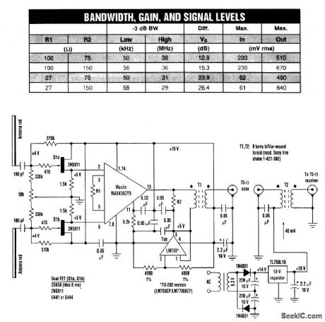
This active antenna acts as a dipole and consists of a dual FET source follower feeding a differential amplifier. The LM759 acts as a virtual ground, splitting the 10-V supply. R1 is a gain set resistor (see table). Dc is fed in via coax cable. The frequency range is 100 kHz to 40 MHz. (View)
View full Circuit Diagram | Comments | Reading(3105)
COMPLEMENTARY_FADER_
Published:2009/7/12 22:03:00 Author:May
Control unit for stage lighting fades out one lamp while simultaneously increasing light output of another with accurate tracking. Gate of silicon controlled rectifier SCR1 is driven by standard external phase control circuit. Interlock network connected to output of SCR1 provides complementary signal for trigger of SCR2. If lamps larger than 150 W are required, use largervalue for C1.-M. E. Anglin, Complementary Lighting Control Uses Few Parts, Electronics, Dec. 12, 1974, p 111; reprinted in Circuits for Electronics Engineers, Electronics, 1977, p 78.
(View)
View full Circuit Diagram | Comments | Reading(611)
CHOKE_CONTROLLED_DIFFERENTIATOR
Published:2009/7/12 22:00:00 Author:May
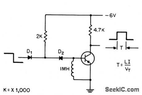
Uses inductance to control on time of transistor.Can also be used as staightforward pulse inverter,Input pulse is wider than output pulse.-W. M. Carey, Using Inducfive Control in Computer Circuits, Electronics, 32:38, p31-33. (View)
View full Circuit Diagram | Comments | Reading(580)
LONG_TURNOFF_DELAY
Published:2009/7/12 21:59:00 Author:May

Combination of timer, optoisolator, and bridge-triggered triac keeps AC motor or other device energized for up to 1 h after control switch is depressed momentarily. Closing of switch drops voltage at pin 2 of timer below 1/3 VCC, making timer output go high and thus tum LED on. At same time, capacitor at pin 7 begins charging. Output re-mains high until oapacitor reaches 2/3 VCC, when outputis reset to low state and motor thereby turned off.-T Mazur,Solid-State Relays Offer New to Soutions to Many Old Problems, EDN Magazine, Nov 20,1973,p 26-32. (View)
View full Circuit Diagram | Comments | Reading(1478)
PULSE_SHAPER_FOR_600_KC_CLOCK
Published:2009/7/12 21:57:00 Author:May


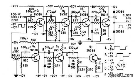
Oscillator input through Q1 switches Q2 on,and same input fhrough Q3 switche Q2 of afer fixed delay, to produce desired rectangular clock pulse.-S.Schoen,Transistors Provide Computer Clock Signals, Electronics, 32:9, p70-72. (View)
View full Circuit Diagram | Comments | Reading(618)
PHASE_SHIFTER
Published:2009/7/12 21:55:00 Author:May
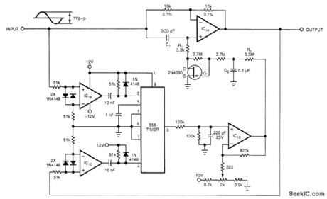
This circuit adds 120 degrees of phase shift to a 50- or 60-Hz input, regardless of the frequency and amplitude fluctuations of that input. The circuit configures a 2N4093 JFET as a voltage-controlled resistor whose value is proportional to the phase difference between the input and the output. The values of C1 R1 and rDS determine the amount of phase shift (120°this case.)A 555 timer implements a phase detector whose two inputs are related to the input and output. The input and output, respectively, drive IC1B and IC1C, which operate as zero-crossing detectors. D1 and D2 limit the positive-going pulse's at the 555 inputs. Thus, the falling edges of IC1B and IC1C's outputs control the 555 timer. The timer's output signal stays low for a time that is proportional to the phase shift between the circuit's input and output.The average value of the timer's output and an offsetting voltage drive IC1D. R2 and C2 filter IC1D's output. The resultant signal controls the JFET. The potentiometer sets the control at a value for which the phase shift between input and output is equal to 120 degrees when the input signal frequency is 50 or 60 Hz. Any differences between the input and output changes the 555 output's average value, thus ultimately modifying the control voltage and the JFET's resistance.To calibrate the circuit, apply a 50-Hz sine wave with an amplitude of less than 1 Vpp to the input and adjust the potentiometer until the phase shift reads 120°on a digital phase meter. For input frequency variations between 40 and 60 Hz, the phase shift changed by a maximum of ±0.17% (equivalent to an offset of only 0.02°/Hz). The average value at IC1D's noninverting input is 3.864 V. (View)
View full Circuit Diagram | Comments | Reading(4808)
PC_WATCHDOG
Published:2009/7/12 21:51:00 Author:May
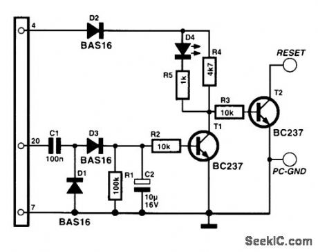
The watchdog is intended to monitor a microprocessor and determine whether it functions correctly or not. It and its software are suitable for use in the background with any PC that runs under DOS or Windows. The hardware is linked to the serial interface, which is then controlled by the software. After the computer has been switched on, the data connections at the serial interface are low.The watchdog software is started at the same time as the selected application program. It provides a permanent rectangular signal at pin 20, which results in C2 being charged and T2 conducting. Pin 4 is made high so that the computer cannot receive a RESET signal. This condition is stable as long as the program runs. If the computer fails (crashes), the rectangular signal falls out and C2 is discharged via R1. This causes T1 to be switched off, whereupon the base of T2 goes high. This transistor is then on and pulls the RESET line of the computer to ground. The computer then restarts. Note that the circuit works only if a computer RESET also causes the serial interface to be reset because that is essential for the high level at pin 4 to be removed. It is only when this pin is at ground level that the RESET pulse is terminated and the cornputer can reboot. (View)
View full Circuit Diagram | Comments | Reading(1222)
40_W_RAPID_START_BALLAST
Published:2009/7/12 21:47:00 Author:May
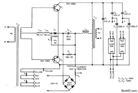
AC line volage is rectified by diode bridge andfiltered by biode bridge and filtered by C6-L1ATransistorsQ1-Q2 with center-tapped tank coil T1A and C1- C3 make up ρower stage of 20-kHz oscillator that develops 600 V P sine wave across T1A. When fluorescent lamps ionize, current to each is limited to about 0.4 A. Lamps operate independently, so one stays on when other is removed Feedback transformer T2A supplies base drive for transistors and filamentpower forlamps Article gives transformer and choke winding data.-R J Haver,The Verdict Is In:Solid-State Fluoresce Ballasts Are Here,EDN Magazine, Nov,5,1976,p 65-69. (View)
View full Circuit Diagram | Comments | Reading(1443)
JOYSTICK_CHANGEOVER
Published:2009/7/12 21:46:00 Author:May
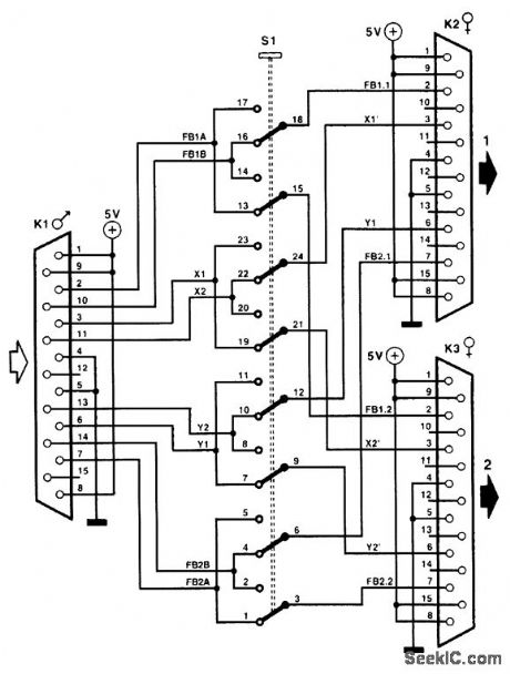
Many I/O cards and sound cards have a standard provision of a 15-way connection for two joysticks. Unfortunately, many programs use the connections for only one joystick. Because often several kinds of joystick are used (in particular, modern flight simulators have provision for very advanced, specialized joysticks), it is frequently necessary to change over connectors. As the joystick connectors are invariably found at the back of the computer, this can be a tedious operation.Moreover, in the long term, it does not do the connectors any good. The present circuit replaces this changing over of connectors by a simple push on a button. In this way, two joysticks can be connected to the computer in a simple and user-friendly way. An eight-pole switch arranges the interconnection of controls X and Y and fire button 1 and fire button 2. (View)
View full Circuit Diagram | Comments | Reading(669)
DISK_READ_WRITE
Published:2009/7/12 21:41:00 Author:May
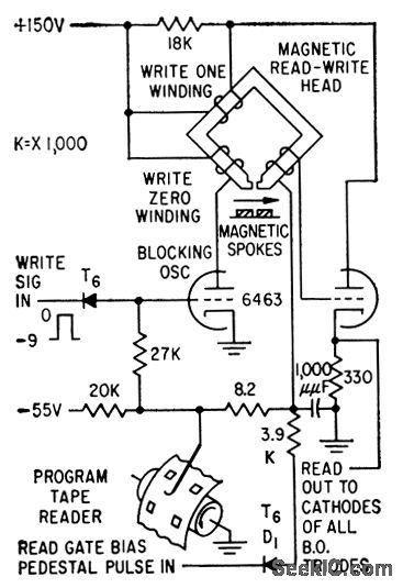
Magnetic head is transformer of twin-triode blocking oscillator circuit used with aluminum disk having radial magnetic spokes that can store from 50 to 100 words.-T. C. Chen and O. B. Stram, Digital Memory System Keeps Circuits Simple, Electronics, 32:11, p130-133. (View)
View full Circuit Diagram | Comments | Reading(657)
RESET_MODE
Published:2009/7/12 21:41:00 Author:May
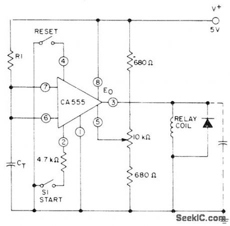
RCA CA555 timer is connected so CT is initiallyheld in discharged stata bytransistor in IC. When start switch is closed, internal flip-flop clears short across CT, driving output voltage high and energizing relay. Voltage across capacitor then increases exponentially with time constant R1CT. When capacitor voltage equals two-thirds of V+, flip-flop resets and discharges capacitor rapidly, driving output low and releasing relay. Timing interval is relatively independent of supply voltage variations. Applying negative pulse simultaneously to reset pin 4 and trigger pin 2 by closing both switches during timing cycle causes timing cycle to restart. Momentary closing of reset switch only serves to discharge CT without restarting timer. - Linear Integrated Circuits and MOS/ FET's, RCA Solid State Division, Somerville, NJ, 19-l7, p 56. (View)
View full Circuit Diagram | Comments | Reading(777)
RS232_TEST_CIRCUIT
Published:2009/7/12 21:40:00 Author:May
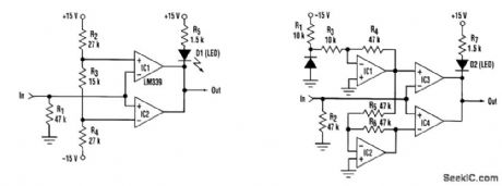
The tester is basically a window comparator, in which the low and high levels are set at +3.0 V and -3.0 V, respectively, by resistors R2, R3, and R4. Resistor R1, when not driven by an RS232 output, will have a low voltage across it (approximately 0 V), and the LED D1 at the output of the comparators is turned off. If the unknown wire of the cable that is tested is an RS232 output, then it will drive the in point to avoltage either between +3 and +12Vor between -3 and -12 V. In both cases, one of the two comparator outputs will be driven low. This turns the LED on, indicating the presence of a wire connected to an,RS232 output. The comparator should be an LM339 type or equivalent (with an open-collector output). The disadvantage of this scheme is that the thresholds are very sensitive to the supply variations. To eliminate this problem, the thresholds at the inputs of the comparators can be created using the normal forward drop on a simple diode and then be brought to the necessary leyels by IC1 (+3 V at its output) and IC2 (a simple inverter). (View)
View full Circuit Diagram | Comments | Reading(1946)
WINDOW_COMPARATORS
Published:2009/7/12 21:39:00 Author:May
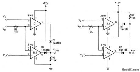
In Fig. 104-3(a), when YIN is between reference voltages VL and VU, output VOUT goes low. If VIN >VL IC2 produces a low. Because IC1 outputs low, if VIN>VU, both outputs are low and VOUT is low. If VIN<VL both IC1 and IC2 are low. Figure 104-3(b) operates the reverse of this; it produces a high when VL<VIN < VU. (View)
View full Circuit Diagram | Comments | Reading(805)
THREE_WIRE_RS232_TO_RS485_CONVERTER
Published:2009/7/12 21:39:00 Author:May
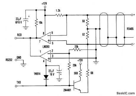


This circuit needs only a minimal three-wire RS232 implementation plus one +10-to +15-V supply voltage to provide a transparent link capable of sending data at transmission rates up to tens of kbaud Circuit operation is as follows∶When both the 232 and the 485 are idle(232 port in MARK state and no 485 device active),the 485 link is held in the 1 state by the 1200-Ω pullup This causesthe top comparator to hold the 232 RCD line negative and therefore in MARK state When a character is transmitted by the 232 port,it begins with a positive-going (SPACE state) START bit on the TXD line,In response, the 2N4401 pulls the - 485 conductor more positive than the + wlre,thustransmitting the START down the 485 cable Meanwhile,the bottom comparator holds the wlre-or (LM393s have opencollector outputs)232 RCD low, blocking the ooodJt port from hearing its own transmission.The recelve side ofthe 232 port remalns idle The rest ofthe bits ofthe character follow along in the same fashion When a character originates somewhere along the 485 bus,it beginswith a 485 transceiver gong active and driving the - line above the + This causes the upper half of the LM393 comparator to release RCD,and this time the bottom comparator doesn't prevent it from being pulled high The data bits are thus allowed to arrlve at the RS232 port,where they appearat standard RS232 bipolar voltage levels,The commonmode voltage range and noise-rejection capabilities of this circuit are compatible with standard 485 specifications The converter's speed is mainly limited by the loading of the comparator outputs because of cable capacitance. (View)
View full Circuit Diagram | Comments | Reading(1758)
SENSE_AMPLIFIER_READS_MEMORY_DATA
Published:2009/7/12 21:36:00 Author:May
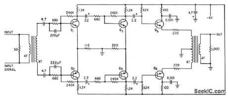
Small signals stored in thin-film momory are amplinfied while rejecting noise from partially selecled bits on same sense line. Circuit is completely isolated differential amplifier operating from low-impedance source.-A.A.Fleischer and E.Johnson, New Digital Conversion Method Provides Nanosecond Resolution, Electronics, 36:18, p55-57. (View)
View full Circuit Diagram | Comments | Reading(547)
RS232_TO_PARALLEL_DATA_CONVERTER
Published:2009/7/12 21:28:00 Author:May

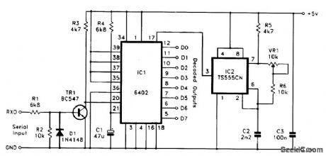
A simple serial decoder circuit based on a 6402 UART (IC1) is shown in the figure. The RS232C input signal is at signal levels of about ±12 V; these must be converted to standard 5-V logic levels before being applied to the serial input of IC1. A simple commonemitter switching stage based on transistor TR1 is used to provide the conversion to normal logic levels, and it also produces the necessary inversion of the input signal. Resistor R4 and capacitor C1 provide IC1 with a positive reset pulse at switch-on. The inputs at pins 35 to 39 program the word format; the method of connection shown in the figure provides a format on 1 start bit, 8 data bits, 1 stop bit, and no parity. Pin 34 is connected to the +5-V rati so that the binary pattem on pins 35 to 39 is loaded into IC1's control register. The decoded bytes of parallel data are available at pins 5 to 12, and pin 4 is connected to the 0 V rail so that these outputs are permanently enabled. In a stand-alone application, the tristate capability of these outputs is not of great value, but, if necessary, this facility can be utilized by applying a control signal to pin 4 of IC1. (View)
View full Circuit Diagram | Comments | Reading(2427)
LOW_COST_WINDOW_COMPARATOR
Published:2009/7/12 21:27:00 Author:May
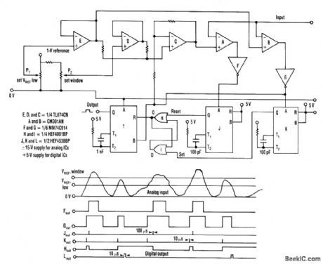
This circuit outputs a TTL-compatible 100-μs pulse whenever the signal falls within the limits set by potentiometers and can be varied to suit the application.Op amps, E, D, and C are used with the two potentiometers to supply reference voltages, derived from a 1-V precision source, for two other op amps (A and B) configured as voltage comparators. The input signal is taken to the negative inputs of both these comparators. C is wired as a noninverting surnming amp, used to derive the higher reference voltage. Consequently, the acceptance window is set. Because the voltage across potentiometer P2 is 0.5V, the window can be set between 0 and 0.5 V above the value chosen for the lower reference value. The lower value is set by P1.The outputs from the comparators are sent to the inputs of inverting Schmitt triggers F and G. Although these triggers operate from a 5-V supply, they have an extended input-voltage range and are capable of handling the comparator's output voltage swings.The two monostables, J and K, are triggered on the rising edge of the Schmitt outputs. J and K set and reset the bistable latch formed by two NOR gates. Latch output Q controls the reset of outputmonostable L, which can only be triggered if its B input goes low, taken from the output of G, while its reset is high.From the timing diagram, when the signal input exceeds the lower reference level, the latch is set and Q goes high. When the higher reference level is exceeded, the latch is reset and Q goes low. If only the lower reference is exceeded, the latch will be set and L is triggered when G's output goes low. When both levels are exceeded, the latch is set, then reset. When G's output goes low, it won't trigger the monostable because its reset is low.The circuit, as shown, was used for a bandwidth-limited, 500- to 5000 Hz input signal with an amplitude range of ±1 V. Modifications can easily be made to cover other frequency and amplitude ranges. (View)
View full Circuit Diagram | Comments | Reading(1053)
CALCULATOR_KEYBOARD_ENTRY_
Published:2009/7/12 21:25:00 Author:May
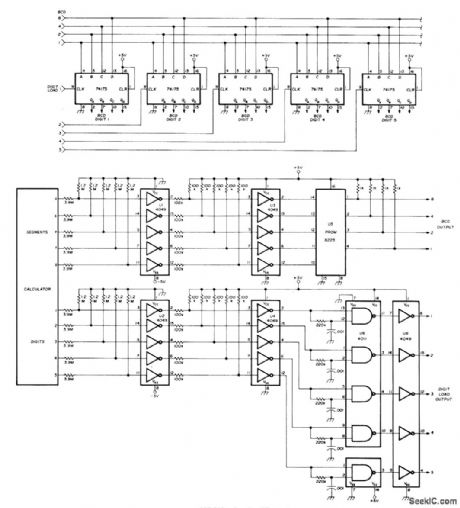
Sampling of signals from inexpensive pocket calculator gives complete data entry system for frequency synthesizer or other application requiring BCD input. Circuit includes contact bounce suppression. Automatic constant feature of TI 1256 calculator used permits storing 0.015 as fixed constant, so frequency goes up 15 kHz (channel spacing on 2 meters) each time + key is pressed.Seven-segment signal normally used for calculator display is decoded by programming 74S188 (8223) PROM, using simplified code conversion table given in article. 74175 ICs provide required demultiplexing of segment data. Articl gives construction details.-B .McNair andG Williman,Digital Keyboard Entry System,Ham Radio, Sept,1978,p 92-97.
(View)
View full Circuit Diagram | Comments | Reading(3600)
WIRELESS_MICROPHONE
Published:2009/7/12 21:20:00 Author:May
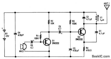
Q1 amplifies the output from an electret microphone MIC1.Audio is fed into oscillator Q2,whichmodulates the signal.LIC1 is a tank circuit for operation in the 88-MHz reglon.The antenna is a 6-to 8-inch ptece of wire.L1 is a variable inductor in the 1-μH range. (View)
View full Circuit Diagram | Comments | Reading(5895)
| Pages:193/471 At 20181182183184185186187188189190191192193194195196197198199200Under 20 |
Circuit Categories
power supply circuit
Amplifier Circuit
Basic Circuit
LED and Light Circuit
Sensor Circuit
Signal Processing
Electrical Equipment Circuit
Control Circuit
Remote Control Circuit
A/D-D/A Converter Circuit
Audio Circuit
Measuring and Test Circuit
Communication Circuit
Computer-Related Circuit
555 Circuit
Automotive Circuit
Repairing Circuit