
Index 206
12V-80V/10A output DC/DC converter voltage stabilization power supply circuit
Published:2011/6/21 22:14:00 Author:TaoXi | Keyword: 12V-80V/10A, output, DC/DC, converter, voltage stabilization, power supply
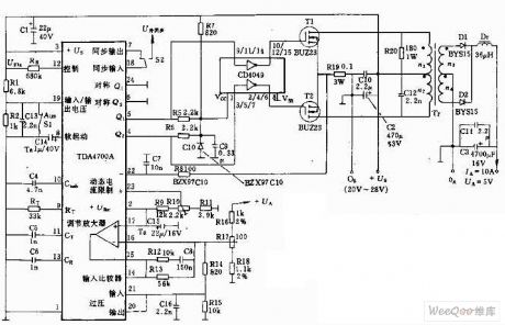
The push-pull type converter circuit uses two BUZ41A SIP MOS transistors and a TDA4718 integrated circuit as the power supply of the ship power grid, the input side and the output side of the converter are isolated. The operating frequency is 50kHz, the efficiency is 75%, the power supply voltage is in the range of 56 to 100V. The output voltage is 12V, and it is rectified by the D10 and D11 full-wave rectifier, at last it is converted by the output filter Dr1, C20, C19 to become the DC.
(View)
View full Circuit Diagram | Comments | Reading(4548)
5V,3A output switch type voltage stabilization power supply circuit
Published:2011/6/22 1:32:00 Author:TaoXi | Keyword: 5V, 3A, output switch, voltage stabilization, power supply circuit
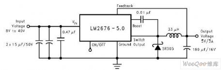
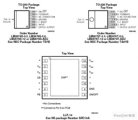
The LM2676 is designed as one kind of switch type integrated voltage stabilizer, it supplies the 3A drive capability, it has all the functions of the step-down switching voltage regulator, also it has good linearity and load regulation characteristics: it gets the high output efficiency by using a low conductivity resistance's DMOS power supply switch; it has the stationary output voltage of 3.3V, 5V and 12V.
The DC stabilized voltage power supply circuit with 8V-40V input and 5V,3A output which is composed of the LM2676 is as shown in the figure.
Pin of the LM2676
(View)
View full Circuit Diagram | Comments | Reading(2086)
Four-phase clock source circuit
Published:2011/6/26 5:31:00 Author:TaoXi | Keyword: Four-phase, clock source circuit
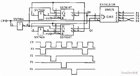
The four-phase clock source circuit is composed of the synchronous mode 4 counter (74107 J-K trigger) and the decoder SN74 LS139. The output of it is the negative pulse, the pulse width is the clock interval.
(View)
View full Circuit Diagram | Comments | Reading(1459)
Pulse source circuit with the presetable pulse number
Published:2011/6/26 3:03:00 Author:TaoXi | Keyword: Pulse source circuit, presetable pulse number
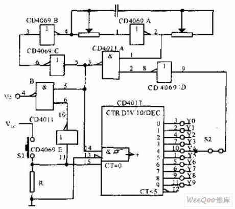
Pulse source circuit with the presetable pulse number is composed of the controllable pulse source and the counter/pulse distributor CD4017. The output pulses is preset by the switch S2. You can clear the counter and blockade the output gate by pressing the start button S1. After the S1 opens, the oscillation source pulse outputs through the NAND gate, and the CD4017 starts counting. When it is the S2's preset position Y, the phase reversal Y controls the oscillation source to stop. So the output pulse number is the preset CP pulse number. In the figure, the switch S2 is in the position that if you press S1, the circuit will output two pulses.
(View)
View full Circuit Diagram | Comments | Reading(625)
Precise 60Hz frequency source circuit
Published:2011/6/25 6:45:00 Author:TaoXi | Keyword: Precise, 60Hz, frequency, source circuit
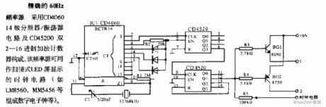
The precise 60Hz frequency source circuit: this circuit is composed of the CD4060 14-stage frequency divider/oscillator circuit and the CD45200 double binary to hexadecimal addition counter. This frequency source can be used in the scanning mode LED screen display clock circuit (such as the digital electric clock which is composed of the LM8560 and MM5456).
(View)
View full Circuit Diagram | Comments | Reading(914)
The regulated circuit composed of LM317
Published:2011/6/24 21:45:00 Author:qqtang | Keyword: regulated circuit
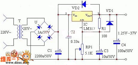
View full Circuit Diagram | Comments | Reading(790)
The time base oscillation source circuit of the digital clock
Published:2011/6/20 9:17:00 Author:Nancy | Keyword: Digital clock, time base , oscillation source

The circuit shown is mainly used as a time base oscillation source of the digital clock. The time base output frequency is 60 Hz, suitable for LED digital clock integrate circuit such as LM8361~LM8365, etc. It is a digital clock crystal oscillator time base circuit formed by the I2 bit binary serial counter/divider CC4040 and hex inverter CC4069. (View)
View full Circuit Diagram | Comments | Reading(1228)
The integrated circuit composed of HA11580
Published:2011/6/24 22:10:00 Author:qqtang | Keyword: integrated circuit
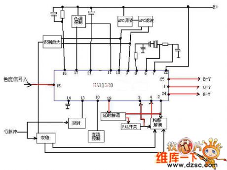
View full Circuit Diagram | Comments | Reading(761)
The 24V regulated power supply of current limiting protection function
Published:2011/6/24 23:16:00 Author:qqtang | Keyword: regulated power supply, current limiting, protection
View full Circuit Diagram | Comments | Reading(730)
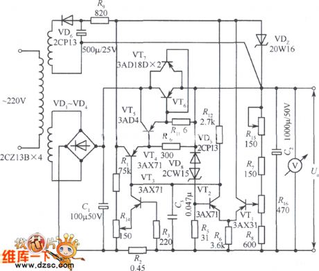
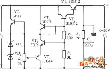
The 0~20v regulated power supply circuit
Published:2011/6/24 23:29:00 Author:qqtang | Keyword: regulated power supply
View full Circuit Diagram | Comments | Reading(699)
25W continuous 28W peak value multi-output power supply circuit
Published:2011/6/19 18:58:00 Author:TaoXi | Keyword: 25W, continuous, 28W, peak value, multi-output, power supply
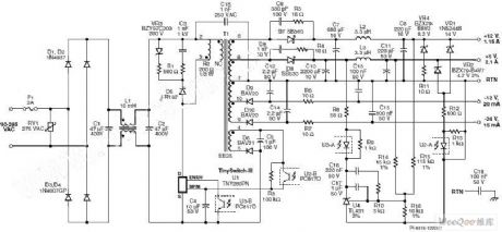
The power supply of the DVD or the set-top box in the figure is designed as the flyback converter with the TNY280PN(U1). In this design, the 10μF capacitance C4 uses the enhanced current-limit point of U1, this point makes the power supply to output the 28W peak power when the device is starting or in the load transient. The 25W continuous 28W peak value multi-output power supply is in every enable switching cycle, the MOSFET of the U1 conducts, the current gets through the primary winding of the transformer T1. When the primary stage current reaches the MOSFET current-limit point, the MOSFET turns off, the energy of the transformer T1 is transmited to the secondary stage. The over-voltage protection is realized by the U2, R12, R13, VR1 and VR2.
(View)
View full Circuit Diagram | Comments | Reading(2634)
Synchronous step-down voltage stabilizer circuit
Published:2011/6/19 9:14:00 Author:TaoXi | Keyword: Synchronous, step-down, voltage, stabilizer
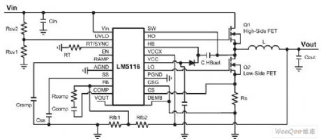
The basic structure of the DC-DC buck regulator circuit is as shown in the figure, this device uses the LM5116 as the pulse width modulator (PWM) switch controller. The critical current path is from the VIN to the output port through the high-side FET; another choose is from the grounding port to the output port through the Rs and the low-side FET. The power loss which is produced along this path is the main loss.
(View)
View full Circuit Diagram | Comments | Reading(1263)
The 28v simple regulated power supply circuit
Published:2011/6/25 2:01:00 Author:qqtang | Keyword: regulated, power supply
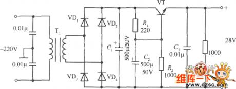
View full Circuit Diagram | Comments | Reading(639)
RCC 5V/400mA switch power supply circuit
Published:2011/6/19 8:01:00 Author:TaoXi | Keyword: RCC, 5V/400mA, switch, power supply

RCC 5V/400mA switch power supply circuit (View)
View full Circuit Diagram | Comments | Reading(3294)
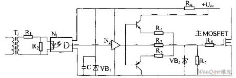
Switch power supply driving circuit
Published:2011/6/16 7:17:00 Author:TaoXi | Keyword: Switch, power supply, driving circuit
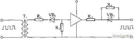
The driving circuit principle diagram:
The switching power supply drivingcircuit:
The main function of the driving circuit is to amplify the variable width pulse which is output by the pulse width controller, so the variable width pulse can be used as the driving signal of the high voltage power switching device. The driving circuit generally has the isolation effect, it usually uses the transformer coupling method to achieve the isolation between the high voltage power switching device's incentive input stage and incentive output stage, and it also exerts the reverse bias to accelerate the turn-off of the device. In the figure, the primary coil input signal of the driving transformer is the output driving signal of the control circuit. (View)
View full Circuit Diagram | Comments | Reading(626)
The soft starting regulated power supply circuit
Published:2011/6/24 7:39:00 Author:Seven | Keyword: soft starting, regulated power supply
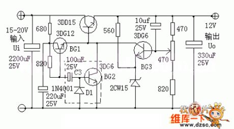
View full Circuit Diagram | Comments | Reading(752)
Positive and negative adjustable voltage stabilization power supply circuit
Published:2011/6/23 7:22:00 Author:Christina | Keyword: Positive, negative, adjustable, voltage stabilization, power supply
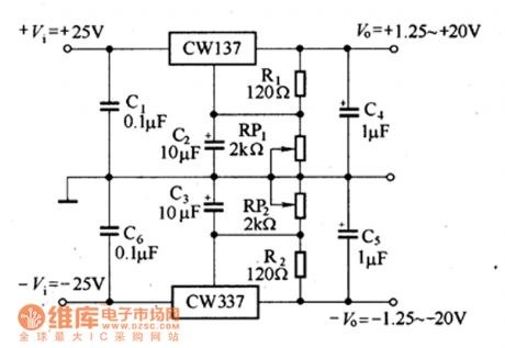
The two-way adjustable voltage stabilization power supply circuit which is composed of the CW317 and CW337 is as shown in the figure.
Positive and negative adjustable voltage stabilization power supply circuit (View)
View full Circuit Diagram | Comments | Reading(832)
The single phase full-wave rectifier circuit
Published:2011/6/17 0:53:00 Author:Seven | Keyword: single phase, full-wave rectifier
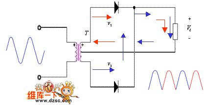
The full-wave rectifier circuit shown in the following figure consists of a transformer with 2 central heads and 2 diodes. Seeing from the circuit, we can find that both the passive and positive half periods has current run across the load, which increase the efficiency.
The features of the full-wave rectifier:The output voltage VO is high; the impulse is low; both the positive and passive half periods can provide current for the load, so the transformer is used fully, and it's efficient.The main parameters:
(View)
View full Circuit Diagram | Comments | Reading(741)
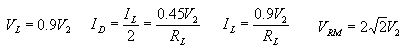
The typical application circuit of 3-terminal IC
Published:2011/6/19 3:03:00 Author:Seven | Keyword: typical application circuit, 3-terminal IC

The fixed typical application circuit of 3-terminal IC is shown in the figure. In the figure, C1 and C2 are used for frequency compensation to avoid self-oscillation and high-frequency noise; C3 is a polymer capacitor, and it can weaken the effect, which is from the low-frequency imported by the power supply, on the output voltage; D is a protection diode, when the input terminal is short, it can offer C3 a discharging circuit to stop the voltage on C3 breaking down the emitter of the regulating device.
The requirement of the 3-terminal regulated IC circuit is: (View)
View full Circuit Diagram | Comments | Reading(615)
Switch integrated voltage-stabilizing circuit
Published:2011/6/21 1:21:00 Author:Christina | Keyword: Switch, integrated voltage-stabilizing
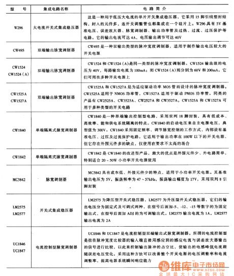
The model numbers and features of some switch integrated voltage-stabilizing circuits are as shown in the table .
(View)
View full Circuit Diagram | Comments | Reading(537)
| Pages:206/291 At 20201202203204205206207208209210211212213214215216217218219220Under 20 |
Circuit Categories
power supply circuit
Amplifier Circuit
Basic Circuit
LED and Light Circuit
Sensor Circuit
Signal Processing
Electrical Equipment Circuit
Control Circuit
Remote Control Circuit
A/D-D/A Converter Circuit
Audio Circuit
Measuring and Test Circuit
Communication Circuit
Computer-Related Circuit
555 Circuit
Automotive Circuit
Repairing Circuit