
power supply circuit
Index 44
Anxiety Symptoms Generator
Published:2012/10/8 2:42:00 Author:muriel | Keyword: Anxiety Symptoms, Generator
Do you want to feel the anxiety symptoms or get rid of your guests?This circuit can be helpful when you want to get rid of your guests (visitors) or feel yourself how anxiety does it feel like. It is a frequency generator that generate a 14 Hertz hum that cannot be heard but will produce a strong anxiety feeling.In order to produce the restlessness you must connect this circuit to an audio amplifier in order to obtain enough sound pressure in the room to get the full impact.You can use the 47K potentiometer to adjust the output level on out 2.Don’t use this anxiety symptoms generator for a long period of time because the long-term effects have not been tested.
Anxiety Symptoms Generator Circuit Diagram
(View)
View full Circuit Diagram | Comments | Reading(845)
Portable Power Supply circuit
Published:2012/9/28 21:05:00 Author:muriel | Keyword: Portable, Power Supply
Here is an ideal Power Supply Unit for trouble shooting the circuit boards. It gives Five and Nine volt regulated DC from a Rechargeable battery. It is portable and handy and can also functions as a Mobile Charger. Transformer less power supply is used in the circuit to charge the battery from mains. This makes the unit compact and light weight. The circuit has two sections. The front end is a charger section with capacitor C1 as the main element. It is an X rated 400 Volt AC capacitor that reduce the 230 volt AC to low volt AC through the Rectance property. Low volt AC is then rectified by the full wave bridge rectifier comprising D1 through D4.
Resistor R1 bleeds the stored current from C1 when the power is disconnected. Resistor R2 reduces the inrush current into the circuit at power on. Rectified AC is then made ripple free by C2 for charging the 9 Volt Rechargeable battery. Zener diode ZD regulates the charging voltage to 15 volts and resistors R3 and R4 gives around 80 to 100 mA charging current. Diode D6 prevents discharge of battery back to the bridge.
Variable resistor VR1 and transistor T1 forms a voltage indicator. LED lights when the battery is fully charged and goes off if the battery voltage reduces below 7 volts. VR1 sets the low voltage level. This prevents deep discharge of battery. When the circuit is connected to mains and S1 is in ON position, battery charges through D5, R3, R4 and D6. When the unit is unplugged from mains, 9 volt output power will be available from the battery. Voltage regulator IC1 gives 5 volt DC. Switch S2 can be used to select 9 v or 5v output.
Portable Power Supply Circuit diagram
Note: Connect a fully charged 9 Volt battery and adjust VR1 till the LED light up. During this adjustment, the circuit should be disconnected from the mains. Use the power supply only after disconnecting it from Mains. The 5volt DC from it can be used for charging the Mobile phone. Use a suitable pin for that. Rechargeable battery can be an ordinary PP3 battery or High current NiMh battery.
(View)
View full Circuit Diagram | Comments | Reading(1653)
Cellphone Charger Using Bike Battery
Published:2012/9/28 21:04:00 Author:muriel | Keyword: Cellphone Charger, Bike, Battery
This is the simple and easy way to tap current from a Motor Bike battery to charge the Mobile Phone. Most of the Mobile Phone battery pack has three 1.2 volt cells making the voltage to 3.6 volts. For fast charging of the battery pack, each cell requires more than 1.2 volts and sufficient current. This circuit can deliver 5 volts at 300 mA to charge the battery quickly. The circuit is Voltage and Current regulated and with Polarity and Surge protection components.
Mobile Charger using Bike Battery Circuit Schematic
The circuit uses a Positive Voltage regulator IC 7805 to give 5 volt regulated output. The components around IC1 are meant for protecting the IC so as to give smooth output power. Zener diode ZD act as the Input Surge protecting diode. It provides 7.2 volts to the input of the regulator IC from the 12 volt bike battery. Diode D1 is the Output Surge and Input Short protecting diode.
When a surge voltage exceeding maximum voltage rating of the regulator is applied to the input or when a voltage in excess of the input voltage is applied to the output, the regulator will be destroyed. If the input terminal shorts with the ground, the output voltage increases above the input voltage(ground potential)and the charge in the capacitor connected to the output flows into the input side which is also fatal to the regulator. Both these situations can be avoided by using the Zener at the input and the diode D1 across the regulator. Capacitor C1 and C2 provide stability to the regulator and these should be soldered close to the legs of the regulator. Capacitor C3 act as a buffer to give constant voltage in the output.7805 Datasheet
7805 IC can tolerate maximum 35 volts and its current rating is 1 Amps maximum. Resistor R1 restricts the charging current to around 330 mA as per the Ohms law. Even if the current is low, charging process will not be affected. Slow charging with 80 to 100 mA current is generally advised. But in case of an emergency, quick charging can be done with high current
Assemble the circuit on a Perfboard and enclose in a small case that can be fitted near the Bike battery. Use suitable pins to connect with the Mobile phone. Charging current can be tapped from the battery using Alligator Clips. Before using the circuit, double check the connections especially the polarity of connectors and measure output voltage and current using a Digital Multi Meter. The same circuit can be used for charging Mobile battery from 12 volt Car battery or from a 12 volt Solar panel.
IC 7805 Pin connection and Alligator Clips
(View)
View full Circuit Diagram | Comments | Reading(1316)
Dual Power source circuit
Published:2012/9/28 21:00:00 Author:muriel | Keyword: Dual, Power source
Here is a Dual power source for the Home Security system which has to be switched on continuously. It is a power saving circuit that uses a Solar panel for providing power during day time and a transformer power supply during night.It has a battery backup and the power to the security system is derived from the 12 Volt 4.5 Ah battery.So that even if the day light is not sufficient in clody days, the security system will work normally. About the Solar Power sourceDuring day time, the security system gets 12 volt power supply from the battery or the Solar Panel. If the amount of power from the solar panel is not sufficient, battery will compensate it. Typically a single solar cell generates 0.5 volt and around 50 mA current in bright light. A single solar cell is rated at 45 mW. So in the 12 volt solar panel, there will be 24 solar cells connected serially. It can give 1 Ampere current in day light. Typically a 15 W Solar panel gives 1 Ampere current in bright light. Here a 12 V 5W Solar panel is used in the circuit to give power to the security system and charging current to the battery. It gives around 300 mA current.
About the DC power source
Night charging is attained by the 12 volt DC obtained from a 0-12 volt 1 Amps step down transformer and the fullwave rectifier comprising D3 through D6. Capacitor C2 removes ripples from DC to give clean power to the security system and for the battery.Resistor R4 gives 80 mA current during night for Trickle charging the battery.At the same time, power to the security system will be available from the battery. The trickle charging provision save AC power and protect battery from over charging since the battery will get sufficient charge during day time.
Dual Power source Circuit diagram
Battery status indicator
This part of the circuit indicates the voltage level in the battery as well as the voltage from the solar panel.Zenerdiode ZD conducts only when the battery holds more than 11.6 volts. When ZD conducts Red LED illuminates.When the battery voltage goes below 11 volts ,LED turns off.If the LED is not lighting, it indicates that battery is not attaining full charge or the solar panel is not giving 12 volts.
LDR switch
This is used to switch on the DC power from the transformer power supply at night. LDR offers low resistance in day light so that it gives more current to the base of T1.It is a PNP transistor and it remains off during day time due high voltage in its base. T2 also remains off due the lack of base bias. During night,resistance of LDR decreases, and the base of T1 becomes negative. It then turns on. T2 also turns on and charging current is available from the emitter of T2. Resistor R4 reduces the charging current to 80 mA for trickle charging the battery. Adjust VR1 to set the sensitivity of LDR.
BD139 and BC557 Pin connections
(View)
View full Circuit Diagram | Comments | Reading(1337)
Fast Charger circuit
Published:2012/9/28 20:57:00 Author:muriel | Keyword: Fast Charger
Here is a High current charger for Fast charging sealed lead acid batteries used in Automobiles, Inverters etc. This charger can give 5 Ampere current for quick rejuvenation of the battery. It uses an Adjustable voltage regulator so that 6 volt and 12 volt batteries can be charged.LM338K is a high current variable voltage regulator that can provide 2 to 25 volts DC with high current output. It’s important features are 7 Ampere peak output current, adjustable output down to 1.2 volts, thermal regulation etc. It is easy to use and require only 2 external resistors to set the output voltage. The time dependent current limiting ability of the device allows peak current of up to 12 ampere to be drawn for short time. So that it is useful in heavy transient loads and speed start up.
LM 338 Variable Regulator
Design considerations
Use of external resistorsLM338 K is available in metal can package TO3. K suffix metal can. It has only two pins – Vin and Adjust. The body of the device acts as the output pin. On the bottom side, the first pin is adjust and the second pin is Vin. LM338 requires heat sink to dissipate heat since it is draining high current. Two resistors are required to set the output voltage. Resistor R1 (220 Ohms) act as the programme resistor. Usually 1.25 volts reference voltage (Vref) develops between the output and adjusts pins. The reference voltage is impressed across the programme resistor R1.The voltage across R1 is constant so that constant current flows through the output set resistor VR1.Therefore output voltage is
Vout = Vref (1 + VR1 / R1) + I Adj VR1
Use of capacitorsTwo capacitors are usually soldered close to the input and output terminals. C2 is the input bypass capacitor. Output capacitor C3 gives stability for the output current.
Circuit operationInput voltage is obtained from a 15-0-15 volt 5 Ampere secondary transformer with rectifying diodes D1 and D2. Capacitor C1 makes the DC ripples free and around 16 volt DC enters into the Vin input of the regulator. VR1 can be used to set the output voltage from 2 volts to 25 volts. A digital panel meter is used for measuring the output voltage. Ready made LED or LCD panel meters are available at reasonable cost. This can be directly connected to the output. So by adjusting VR1, it is easy to see the output voltage in the meter .If the output put voltage reduces due to line voltage drop, it can be easily detected through the panel meter. The panel meter also can be used to measure the terminal voltage of the battery. If the power supply is switched off, meter shows the terminal voltage. If the voltage remains steady, it indicates that the battery is fully charged and holding charge.Easily available IN 5402 diodes are rated at 3 Amps so if the device become too hot, use a 10 A KBPC 1000 Bridge rectifier.
Fast Charger Circuit diagram
(View)
View full Circuit Diagram | Comments | Reading(1331)
Transformerless Power Supply 30V 1A
Published:2012/9/28 20:56:00 Author:muriel | Keyword: Transformerless, Power Supply, 30V, 1A
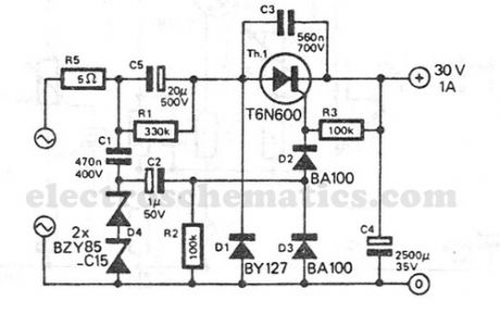
This transformerless power supply circuit is designed for medium current applications. During the negative half period, the capacitor C5 is charged to peak voltage network.
Transformerless Power Supply Circuit Schematic
The positive half wave will open the thyristor and the electric charge accumulated in C5 will be transferred in C4. The transport of electric charge through the thyristor begins when the voltage on C4 drop below a specified level of voltage (set by zener D4). Thus the output voltage does not depend too much on the voltage variations or the output load.
The thyristor control signal is obtained as follows: main sinusoidal voltage is applied through capacitor C1 to D4 zener diodes that limit the voltage to 30 Vpp. Thyristor will trigger on the first front of the limited voltage that is applied through C2 – R2. (View)
View full Circuit Diagram | Comments | Reading(3981)
Capacitor Power Supply circuit
Published:2012/9/28 20:46:00 Author:muriel | Keyword: Capacitor, Power Supply
One of the major problems that is to be solved in an electronic circuit design is the production of low voltage DC power supply from Mains to power the circuit. The conventional method is the use of a step-down transformer to reduce the 230 V AC to a desired level of low voltage AC. The most simple, space saving and low cost method is the use of a Voltage Dropping Capacitor in series with the phase line.
Capacitor Power supply Circuit
Selection of the dropping capacitor and the circuit design requires some technical knowledge and practical experience to get the desired voltage and current. An ordinary capacitor will not do the job since the device will be destroyed by the rushing current from the mains. Mains spikes will create holes in the dielectric and the capacitor will fail to work. X-rated capacitor specified for the use in AC mains is required for reducing AC voltage.
X Rated capacitor 400 Volt
(View)
View full Circuit Diagram | Comments | Reading(1366)
Snap Action Relay circuit
Published:2012/9/27 21:40:00 Author:muriel | Keyword: Snap Action, Relay
When a Relay driver circuit is used in Sensor based electronic circuits, false triggering may occurs due to unwanted relay clicking. The input signal level is not sharp in most sensor circuits and the transition stages are slow. So the relay driver transistor partially turns on / off . The relay coil will not become fully energized leading to vibration of the relay contacts and heating. A Snap Action relay driver with Schmitt trigger action can eliminates this.
The diagram below is the relay driver circuit with Snap Action for the clean switching of the relay. When the input signal at the base of T1 decreases, it turns off allowing T2 to conduct by giving base current through R3.When T2 conducts, its emitter current increases and this raises the voltage at the emitter of T1.This rapidly reduces the base current of T1 and it switches off rapidly. When T1 turns off rapidly, T2 turns on faster and relay energize. This snap action reduces the time gap between the working of T1 and T2 and prevents relay chattering.
Snap Action Relay Circuit
Note: The value of R2 must be higher than the resistance of the Relay coil to give more current through R5 when T2 turns on and less flow when T1 turns on. (View)
View full Circuit Diagram | Comments | Reading(970)
78XX Voltage Regulator circuit
Published:2012/9/27 21:37:00 Author:muriel | Keyword: 78XX, Voltage Regulator
IC 78XX Series includes three terminal positive voltage regulators commonly available in TO 220 package. These are useful in wide range of applications to give precise output voltage. These regulators have internal current limiting, and thermal shutdown circuitry etc. If good heat sinking is provided, these ICs can deliver 1 Amps current. These are generally considered as fixed voltage regulators but their functions can be manipulated to convert them into variable voltage regulators78 XX REGULATOR IC
.
The important parameters of 78 XX series are1. Maximum output current 1.5A2. Output voltages – 5,5.2,6,8,9,10,12,15,18,24volts3. Thermal overload protection4. Short circuit protection
The following circuits give an idea about the input voltage at which the IC gives precise output. Fig 1 and 2 shows the conditions in which the IC7805 is giving precise 5 volt output. 7805 IC requires minimum 6.5 volts to give 5 volt output. To monitor this, a Zener and LED are included at the input. Zener voltage is 4.7 volts and the forward voltage drop of the ordinary diffuse type Red LED is 1.8 volts. When the input voltage is above 6.5 volts (4.7+1.8), Zener conducts and LED turn on. This indicates that IC is getting input voltage above 6.5 volts. When the input voltage reduces below 6.5 volts, Zener cut off and LED turns off.
7805 Circuit 1
Fig 2 shows another LED indication. The brightness of LED reduces as the input voltage reduces below 6.5 volts.
(View)
View full Circuit Diagram | Comments | Reading(1291)
Homemade PCB
Published:2012/9/27 21:32:00 Author:muriel | Keyword: Homemade, PCB
Printed circuit board or PCB is one of the important things to assemble an electronic circuit. It provides support to the components and makes electrical connection between the parts. In PCB assembling, the components are placed on one side of the Copper laminate passing their pins or leads to the other side through the holes. The pins/leads are then soldered to connect with the PCB tracks. Here explains the easiest method to make a homemade PCB for prototyping.To make the PCB, following materials are required
1. Copper clad boardThis is available in different sizes. Select a suitable size to accommodate all the components. If the copper clad board is large in size, cut it to the required size using a Hacksaw blade. The copper clad board has a copper coated side which forms the soldering side. The other side is the component side on which the components are placed.If there is any dirt or copper oxide on the copper side, clean it throughly using a pencil eraser
Copper clad board
2. Ferric chloride solutionThis is the Etching solution of Ferric chloride. It removes the unwanted copper layers from the copper clad board. The Etching solution can be prepared by dissolving 50 gms Ferric chloride powder in 100 ml Luke warm water.
3. PCB drill and bits
PCB drill is used to drill holes in the PCB. A hand drill with suitable bits is sufficient for the purpose. Use drill bits of the following size to make holes for different components
A. 1mm – for IC pinsB. 1.2mm – for Resistor, capacitor, transistor etc.C. 1.5mm – for diode, LED pins, presets etc.D. 5mm – for LED, nuts, screws etc.E. 8mm – for switches, pots etc.
4. OHP Permanent Marker Pen, Tracing / Butter paper, Pencil Carbon paper, Varnish etc.
PCB Making
PCB making involves the following stages1. Draw the circuit diagram as compact as possible on a paper. Mark the points (component pins) to be drilled. This diagram is used for Pattern drawing on the copper clad board.
2. Draw the same diagram in the tracing / butter paper using the OHP marker pen. Draw the diagram carefully without any overlapping or shorting of tracks or components. The neatness of the PCB lies in the Pattern drawing. After drawing, see the other side of the paper. There is a Mirror Sketch of the tracks. This is the actual pattern of the PCB.
Mirror Sketch of PCB tracks
3. Place the Pencil carbon on the copper side of the copper clad board. The ink side of the carbon paper should face the copper layer.
4. Place the tracing paper with diagram over the carbon paper. The diagram should be in the middle part of the copper clad board. Fold the sides of the tracing and carbon papers and stick it using cello tape. This prevents the movement while drawing.
5. Once again redraw the diagram using the OHP marker pen so that the carbon ink will create a mirror sketch on the copper clad board.
6. Remove the tracing paper and carbon paper. Using the OHP marker pen, redraw the carbon pattern of the mirror sketch on the copper laminate. So that the tracks will be created using the permanent marker ink. Keep it for 10 minutes to dry the ink.
7. Mark points to be drilled. (View)
View full Circuit Diagram | Comments | Reading(1036)
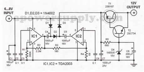
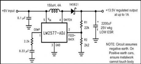
6v to 12v converter circuits
Published:2012/9/27 21:19:00 Author:muriel | Keyword: 6v to 12v, converter
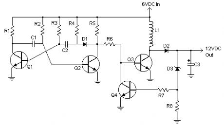
Here are some of 6v to 12v converter circuits that can be used to convert a small voltage of about 6 volts to a higher voltage of 12 volts but ofcourse with a lower current rating.
6 volts to 12 volts converters
This inverter circuit can provide up to 800mA of 12V power from a 6V supply. For example, you could run 12V car accessories in a 6V car. The circuit is simple, about 75% efficient and quite useful. By changing just a few components, you can also modify it for different voltages.
Source: http://www.aaroncake.net/circuits/6-12conv.asp
Parts List:R1, R4 - 2.2K 1/4W ResistorR2, R3 - 4.7K 1/4W ResistorR5 - 1K 1/4W ResistorR6 - 1.5K 1/4W ResistorR7 - 33K 1/4W ResistorR8 - 10K 1/4W ResistorC1,C2 - 0.1uF Ceramic Disc CapacitorC3 - 470uF 25V Electrolytic CapcitorD1 - 1N914 DiodeD2 - 1N4004 DiodeD3 - 12V 400mW Zener DiodeQ1, Q2, Q4 - BC547 NPN TransistorQ3 - BD679 NPN TransistorL1 - See Notes on the websiteMISC - Heatsink For Q3, Binding Posts (For Input/Output), Wire, Board
This 6V to 12V converter circuit is made with an IC from SGS with several additional components. The IC is a TDA2003 but it can be replaced with a TDA2002.The cost of building the 6volts to 12 volts converter should be low enough to justify constructing it instead of modifying the entire equipment setup to work directly with a 6 volts power supply. The two principles of simplicity and functions properly without the need of the transformer.
Source: http://apowersupply.com/6v-to-12v-converter-tda2003-144.html
This is a Simple Switcher step-up voltage regulator made by National Semiconductor, (part number LM2577-ADJ). Together with a few extra components, a heat sink and some wiring, it is possible to generate over 1A from the battery of an Austin. The output connector is taken from a car charger extension lead, so that a phone or a sat-nav just plugs straight in.Source: http://www.austin7.org/6v_to_12v_converter.htm (View)
View full Circuit Diagram | Comments | Reading(3107)
12 Volts Transformerless Power Supply
Published:2012/9/26 21:24:00 Author:muriel | Keyword: 12 Volts, Transformerless, Power Supply
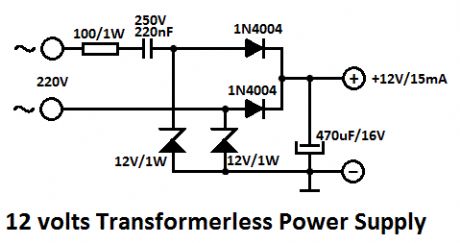
This 12 Volts transformerless power supply take advantage of the fact that a Zener diode is also a normal diode that conducts current in the forward direction. During one half wave, the current ?ows via D1 through the load and back via D4, while during the other half wave it ?ows via D3 and D2. Bear in mind that with this circuit (and with the bridge rectifier version), the zero voltage reference of the DC voltage is not directly connected to the neutral line of the 230-V circuit.
Transformerless Supply Circuit Schematic
(View)
View full Circuit Diagram | Comments | Reading(1672)
5V Switch-Mode Power Supply circuit
Published:2012/9/26 21:24:00 Author:muriel | Keyword: 5V, Switch-Mode, Power Supply
This 5 volts Switch Mode Power Supply circuit use the IC from National Semiconductor has been producing and designing ICs for use in switch-mode power supplies for many years. The application of these devices is normally straightforward, helped by the excellent documentation that is available. A typical example of a switch-mode power supply is that based on the LM2671 or LM2674.The components for it are available for outputs of 3.3 V, 5 V and 12 V. There is also a version providing a presettable output voltage. Within the specified application, the supplies can deliver currents of up to 500 mA. Note-worthy is the high switching frequency of 260 kHz.
This has the advantage that only low-value inductor and capacitors are needed, and this results in excellent efficiency and small dimensions. In normal circumstances, the efficiency is 90% and may even go up to 96%. Both ICs provide protection against current and temperature overloads.
The LM2671 has a number of additional facilities such as soft start and the option to work with an external clock. The latter enables several supplies to be synchronized so as to give better control of any EMC (ElectroMagnetic Compatibility). The application shown in the diagram provides an output voltage of 5 V and an output current of up to 500 mA. Diode D1 is a Schottky type ((Uco≥ 45 V and Imax≥ 3 A).
5 volts switch mode power supply
(View)
View full Circuit Diagram | Comments | Reading(1274)
Retriggerable Monostable Circuit
Published:2012/9/25 21:39:00 Author:muriel | Keyword: Retriggerable, Monostable Circuit
CD 4047 is the low power Monostable / Astable Multivibrator that requires only an external capacitor and a resistor to give the output pulses.The values of these components determine the output pulse width in the Monostable mode and output frequency in the Astable mode.Monostable mode
Monostable mode can be obtained by triggering the + input of the IC using a low to high pulse or by a high to low pulse at the – input. The IC can be retriggered by applying simultaneous low to high pulse in both the + and – inputs.
Astable mode
This can be obtained by keeping a high / low level at the Astable input. Output frequency depends on the timing components.
Pin connections of CD4047
CD 4047 is a low power CMOS IC that can operate between 3 to 15 volts DC.
Retriggerable Monostable Circuit diagram
(View)
View full Circuit Diagram | Comments | Reading(1003)
Voltage Stabilizer circuit with LDR (photoresistor)
Published:2012/9/25 21:37:00 Author:muriel | Keyword: Voltage Stabilizer, LDR, photoresistor
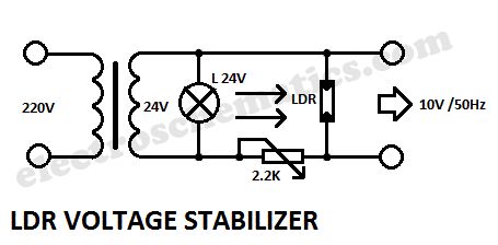
This is a very interesting a.c. voltage stabilizer that uses a LDR or photoresistor to stabilize an alternating current (AC).If the voltage increases then the brightness of the light bulb increases too and the LDR’s resistance will decrease. If the potentiometer is properly adjusted then the AC voltage will stay constant.
The optimal adjustment of potentiometer is done experimental, feeding the circuit with a variable ratio transformer, which can simulate variations of voltage network.
LDR voltage stabilizer circuit schematic
(View)
View full Circuit Diagram | Comments | Reading(1434)
Simple 12 Volt Charger circuit
Published:2012/9/25 21:27:00 Author:muriel | Keyword: 12 Volt, Charger
This is the circuit of a simple 12 volt battery charger for Lead Acid battery. It gives 12 volt and 5 Amps current for quick charging of the battery. If the battery is partially discharged, full charge will be attained in one hour.The circuit uses a 0-14 volt 5 Ampere Step down transformer and a 10 Amps Bridge rectifier module to convert AC to DC. Since pulsed DC is good for Lead Acid battery, a low value smoothing capacitor is used as C1.To monitor the charging status, Ampere meter is provided in the positive rail. LED act as the Charger on status.
Simple 12 Volt Battery Charger Circuit
When the output is connected to the battery terminals, the meter shows a higher reading depending on the current flow into the battery. As the battery attains full charge, its terminal voltage rises to 13.8 volts and current through the meter ceases. The meter reading then returns to zero. This indicates the full charge state and the charging can be terminated. (View)
View full Circuit Diagram | Comments | Reading(1389)
Charger On Demand
Published:2012/9/25 21:27:00 Author:muriel | Keyword: Charger
This Automatic Battery charger turns On only when the battery demands charging current. It can be used to charge 12 Volt Lead Acid or Tubular batteries .The automatic switching helps to keep the battery always in top condition. The overcharge and over discharge cut off facilities are included so that the charger can be left unattended for long periods.
The switching action through the relay is achieved by by sensing the terminal voltage of the battery under charge. Relay contacts break the AC supply to the charger transformer when the battery voltage rises above 14 volts. When the terminal voltage drops below 11.5 volts, relay contacts complete the Neutral path of AC supply to the charger transformer.
Operational Amplifier IC1 is used as a precision voltage comparator to monitor the voltage level of the battery. Its Inverting input gets a reference voltage of 1.8 V from the junction of Red LED and R3 while the Non inverting input gets slightly higher voltage of 2 volts ( as set by VR1). This makes output of IC1 high. PNP transistor then remains off to keep the relay de-energized. Since the Neutral line is connected through the Comm and NO contacts of the relay, AC path remains cut off and no charging takes place.
When the battery voltage drops below 11.5 volts, voltage at the Non inverting input (pin3) drops below that of the Inverting input (pin2) and the output of IC1 turns low. T1 then conducts to actuate the relay. Relay contacts completes the neutral path and charging process starts. Green LED indicates the charging process.
Charger On Demand Circuit
(View)
View full Circuit Diagram | Comments | Reading(1112)
Day Charger circuit
Published:2012/9/25 21:27:00 Author:muriel | Keyword: Day, Charger
This LDR controlled Adjustable charger can be used to charge the Rechargeable battery of portable devices. It charges the battery only during day time. This saves energy and prevents overcharging of the battery. The output voltage from the charger varies from 6 – 12 volts which can be adjusted. Current flow depends on the ambient light in the room.Charging current is obtained from a 0-12 volt 500 mA step-down transformer, a full wave rectifier D1through D4 and smoothing capacitor C1. LED indicates the power on status. LDR is used as a light sensitive switch for controlling the charging process. During day time, LDR offers less resistance and provides sufficient base bias to T1. When T1 conducts, output will be available from the emitter of T1.Pot VR1 controls the output voltage. Current flow depends on the resistance of LDR which in turn depends on the light falling on LDR. In bright day light, resistance of LDR reduces to 100 K or less and more current flows into the base of T1. When the LDR is in dark, its resistance increases to 10 Meg Ohm and prevents the base current to T1. T1 then turns off and output ceases.
Day Charger Circuit
Note: Keep the LDR / charger in a place where day light is available. Adjust VR1 till sufficient output voltage is obtained. Measure the output using a multimeter. Output current can be between 50 mA to 300 mA depending on the illumination. If continuous charging is required, replace LDR with a 470 ohms resistor.
(View)
View full Circuit Diagram | Comments | Reading(681)
Solar Power System Guard
Published:2012/9/25 1:01:00 Author:muriel | Keyword: Solar Power,System,Guard
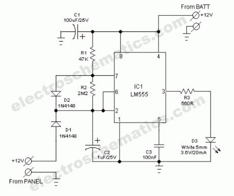
The common home solar power system, in principle consists of a roof-mounted solar panel, a charge controller and a storage battery bank plus direct or electronic inverter powered electric lighting units. In some situations, the solar panel is mounted on a mast extended from ground and this may become an obstacle during night time.Here, ultra simple circuit of an obstacle indicator is presented. Just assemble the circuit on a piece of general-purpose circuit board and then enclose it in small ABS box. Next, attach the unit on the solar panel mast using suitable clamps. This little circuit takes power from the 12V battery of the solar system and switch on a blinking white light spot, when dc power supply from the solar panel is absent, ie at night time!The solar power system guard circuit is a gated astable multivibrator wired around the”evergreen” tiny timer chip LM555(IC1). The thing that makes this design special is the ultra-low current consumption. The white clear glass type LED (D3) flashes only very briefly each time with a duty cycle near 10%. The circuit is gated through diode D1 such that the flashing only begins when sufficient supply from the solar panel is absent.
Solar Power Illumination System Circuit
(View)
View full Circuit Diagram | Comments | Reading(2279)
PC Power Box with E-fuse
Published:2012/9/25 0:52:00 Author:muriel | Keyword: PC,Power Box

This little circuit will help you to remove all surplus small ac mains adaptors from your desktop. The circuit is nothing, but a smart dc power box directly powered by the smps of your desktop personal computer. Regulated, clean and protected +12VDC is available at the output of this unit. In addition, a USB power port is provided to re-charge portable devices including cellphones and music players, etc.How does the pc power box worksAll you need is to open your system box and connect an unused 4-pin drive power connector from the system smps to this circuit. +12V (Yellow wire) from the smps is processed by a resettable electronic fuse built around components T1, T2 and T3 and feed to the output terminal. Similarly the +12V is down converted to stable +5V by fixed 3 pin regulator IC1.As a result, +12V (500 -750mA max, based on the electrical characteristics of T2 used) and +5V (1A max) DC supplies are available for external use, without affecting the normal pc functions. Switch S1 is the power on/off cum reset switch. Resistor R3 sets the maximum allowable output current rate and T1 disables the output power switch T3, when output load current exceeds the set value.
Smart dc power box circuit schematic
(View)
View full Circuit Diagram | Comments | Reading(1508)
| Pages:44/291 At 204142434445464748495051525354555657585960Under 20 |
Circuit Categories
power supply circuit
Amplifier Circuit
Basic Circuit
LED and Light Circuit
Sensor Circuit
Signal Processing
Electrical Equipment Circuit
Control Circuit
Remote Control Circuit
A/D-D/A Converter Circuit
Audio Circuit
Measuring and Test Circuit
Communication Circuit
Computer-Related Circuit
555 Circuit
Automotive Circuit
Repairing Circuit