
power supply circuit
Index 43
Triangle and Squarewave Generator
Published:2012/10/18 2:15:00 Author:muriel | Keyword: Triangle, Squarewave, Generator
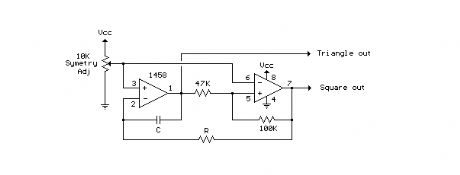
Here is a simple triangle/squarewave generator using a common 1458 dual op-amp that can be used from very low frequencies to about 10 Khz. The time interval for one half cycle is about R*C and the outputs will supply about 10 milliamps of current. Triangle amplitude can be altered by adjusting the 47K resistor, and waveform offset can be removed by adding a capacitor in series with the output.
(View)
View full Circuit Diagram | Comments | Reading(1114)
Low Frequency Sinewave Generators
Published:2012/10/18 2:09:00 Author:muriel | Keyword: Low Frequency, Sinewave Generators
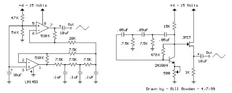
The two circuits below illustrate generating low frequency sinewaves by shifting the phase of the signal through an RC network so that oscillation occurs where the total phase shift is 360 degrees. The transistor circuit on the right produces a reasonable sinewave at the collector of the 3904 which is buffered by the JFET to yield a low impedance output. The circuit gain is critical for low distortion and you may need to adjust the 500 ohm resistor to achieve a stable waveform with minimum distortion. The transistor circuit is not recommended for practical applications due to the critical adjustments needed.
The op-amp based phase shift oscillator is much more stable than the single transistor version since the gain can be set higher than needed to sustain oscillation and the output is taken from the RC network which filters out most of the harmonic distortion. The sinewave output from the RC network is buffered and the amplitude restored by the second (top) op-amp which has gain of around 28dB. Frequency is around 600 Hz for RC values shown (7.5K and 0.1uF) and can be reduced by proportionally increasing the network resistors (7.5K). The 7.5K value at pin 2 of the op-amp controls the oscillator circuit gain and is selected so that the output at pin 1 is slightly clipped at the positive and negative peaks. The sinewave output at pin 7 is about 5 volts p-p using a 12 volt supply and appears very clean on a scope since the RC network filters out most all distortion occurring at pin 1.
(View)
View full Circuit Diagram | Comments | Reading(1117)
FM modulator circuit
Published:2012/10/11 21:08:00 Author:muriel | Keyword: FM modulator
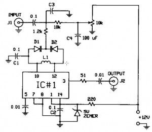
The FM modulator circuit (frequency modulation) is built with a Motorola MC1648P oscillator. Two varactors, Motorola MV-209 are used to frequency modulate the oscillator. The 5000 Ω potentiometer is used to bias the varactors for the best linearity. The output frequency of approximately 100 MHz can be adjusted by changing the value of the inductor.
The output frequency can vary as much 10 MHz on each side. The output level of the modulator is -5 dBm. In this fm modulator prototype the varactor bias was 7.5V for the best linearity but this could be different with other varactors.
FM modulator circuit diagram
(View)
View full Circuit Diagram | Comments | Reading(3150)
DC voltage regulator circuit
Published:2012/10/11 2:33:00 Author:muriel | Keyword: DC voltage, regulator
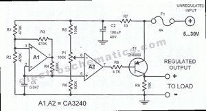
This circuit regulates a DC power output. It has a very wide application range. It can be used to control the speed of a motor, a pump, a toy train, the brightness of a LED or lamp, etc. Practically, it can be used in any application that uses a regulated DC power with pulse width modulation (PWM). It was originally used as a jumbo LED dimmer.The circuit works this way: the A1 opamp functions as a square wave generator. At its non-inverting input is a by product triangle wave signal. The IC A2 following it functions as a simple comparator. A reference voltage is fed to the inverting input of the A2 IC via the potentiometer P1. The output of A2 is a square wave signal with a constant frequency of around 200 Hertz. This signal has a variable pulse width from 0 to 100%.
DC regulator circuit diagram
(View)
View full Circuit Diagram | Comments | Reading(1523)
9V battery indicator circuit
Published:2012/10/11 2:30:00 Author:muriel | Keyword: 9V, battery indicator
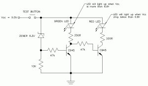
This is a very simple 9V low battery indicator circuit which has 2 LEDs, one green which will light up when the battery voltage is higher than 6.9 volts and one red LED which will light up when the battery voltage is bellow 6.9 volts. You can use BC547 … BC549 .
Low battery indicator circuit diagram
(View)
View full Circuit Diagram | Comments | Reading(2639)
Adjustable Variable power supply
Published:2012/10/11 2:22:00 Author:muriel | Keyword: Adjustable Variable, power supply
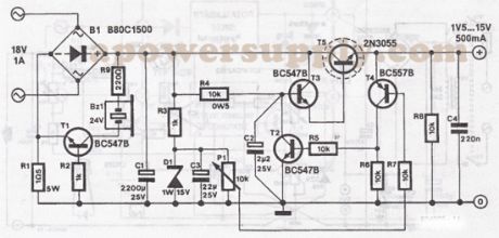
aPowerSupply.com has published a good variable power supply circuit schematic which can be adjusted between 1,5 V and 15 V with a 500 mA maximum current.It uses the well known 2N3055 transistor in a Darlington configuration.
Adjustable power supply circuit diagram
(View)
View full Circuit Diagram | Comments | Reading(1453)
LM7805 voltage regulator
Published:2012/10/11 2:22:00 Author:muriel | Keyword: LM7805, voltage regulator
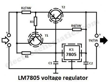
Voltage regulator IC’s, with 3 pins, from LM7805 and LM7812 series are excellent for usage in voltage regulator circuits. If you need higher currents, up to 3 A, you must add a complementary transistor, T2 in this schematic. In a normal design, in case of a shortcircuit, the power dissipation can be very high. This problem can be solved using the voltage regulator design presented on aPowerSupply.com – voltage regulator circuit.
7805 voltage regulator circuit diagram
(View)
View full Circuit Diagram | Comments | Reading(5282)
Power status indicator circuit
Published:2012/10/10 21:45:00 Author:Ecco | Keyword: Power status, indicator
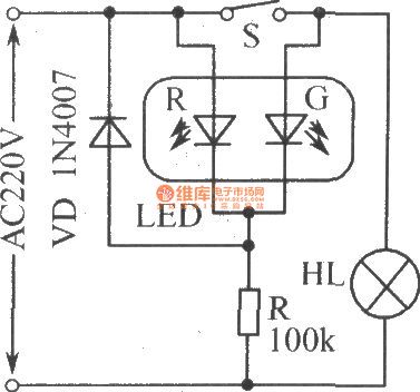
As shown in the figure, LED - R is used for power source directions, LED-G is used for working condition indicator of the load HL ( lamp ). When 220V AC mains is normal, LED - R emits red light. When switch S is closed, HL also emitting light, LED-G emits green light, because the LED-R also emits light at this time, bicolor LED emits orange-red light when S is closed.
(View)
View full Circuit Diagram | Comments | Reading(2132)
Transformer Less Power Supply 12V 100mA
Published:2012/10/10 1:48:00 Author:muriel | Keyword: Transformer, Less Power Supply, 12V, 100mA
This is a transformerless power supply for low current applications. C1 is the X rated AC capacitor that reduces high volt AC. D1-D4 rectifies AC to DC and C2 removes ripples. R1 is the bleeder to remove stored current in AC when power is off. R2 limits inrush current. A Zener can be used in the output to get regulated DC.
Transformer Less Power Supply Circuit Diagram
(View)
View full Circuit Diagram | Comments | Reading(1469)
Mobile Phone Travel Charger
Published:2012/10/10 1:46:00 Author:muriel | Keyword: Mobile Phone, Travel Charger
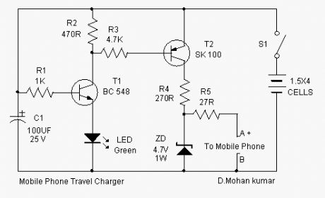
Here is an ideal Mobile charger using 1.5 volt pen cells to charge mobile phone while traveling. It can replenish cell phone battery three or four times in places where AC power is not available.Most of the Mobile phone batteries are rated at 3.6 V/500 mA. A single pen torch cell can provide 1.5 volts and 1.5 Amps current. So if four pen cells are connected serially, it will form a battery pack with 6 volt and 1.5 Amps current. When power is applied to the circuit through S1, transistor T1 conducts and Green LED lights.
When T1 conducts T2 also conducts since its base becomes negative. Charging current flows from the collector of T1. To reduce the charging voltage to 4.7 volts, Zener diode ZD is used. The output gives 20 mA current for slow charging. If more current is required for fast charging, reduce the value of R4 to 47 ohms so that 80 mA current will be available. Points A and B are used to connect the charger with the mobile phone. Use suitable pins for this and connect with correct polarity.
Mobile Phone Travel Charger Diagram
(View)
View full Circuit Diagram | Comments | Reading(1645)
DC Voltage Doubler Circuit with 555
Published:2012/10/9 2:40:00 Author:muriel | Keyword: DC Voltage, Doubler, 555
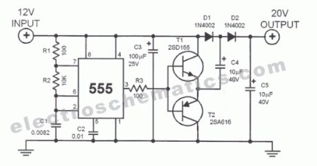
This dc voltage doubler circuit produces a voltage that is twice its voltage supply. This is useful when a higher voltage level is needed out of a single lower voltage power supply. Since the current consumption levels are low in such cases, the circuit can be built with minimal resources.
Voltage Doubler Circuit Schematic
The electronic circuit is basically a square wave generator using the common LM555 timer IC. It is followed by a final stage made of transistors T1 and T2. The actual doubler circuit is made of D1, D2, C4 and C5 components.
The 555 dc voltage doubler timer IC works as an astable multivibrator and generates a frequency of about 8.5 kHz. The quare wave output drives the final stage made of T1 and T2. This is how the doubler works: by a low amplitude of the signal, transistor T1 blocks while T2 conducts. The minus electrode of the capacitor C4 is grounded and charges through D1. By a high amplitude of the signal, transistor T1 conducts while T2 blocks. However, capacitor C4 cannot discharge because it is blocked by D1. The following capacitor C5 is therefore charged with a combined voltage from C4 and the power supply (12V input).On standby, the circuit delivers around 20 volts The maximum load must not exceed 70 mA. The actual output voltage is around 18 volts giving an efficiency rating of 32 %. On lower current ratings, the voltage is higher. If a stable voltage lever is desired, a 3 pin voltage regulator IC can be added at the output. The regulator IC’s own current consumption must be added to the total current consumption which must not exceed 70 mA.For more voltage doublers check the related posts bellow.
(View)
View full Circuit Diagram | Comments | Reading(3030)
Power supply 4-30V 20A LM338
Published:2012/10/9 2:39:00 Author:muriel | Keyword: Power supply,4-30V, 20A, LM338
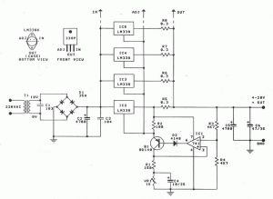
This is a regulated and adjustable power supply which can deliver up to 20A and adjustable voltage between 4 and 30V. It is easy to build and uses LM338 and 741 integrated circuits. VR1 it is used to adjust the output voltage.
LM338 power supply circuit schematic
(View)
View full Circuit Diagram | Comments | Reading(2872)
Solar Charger Circuit
Published:2012/10/9 2:32:00 Author:muriel | Keyword: Solar Charger
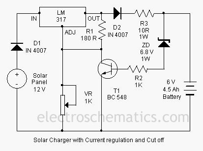
Here is a solar charger circuit that is used to charge Lead Acid or Ni-Cd batteries using the solar energy power. The circuit harvests solar energy to charge a 6 volt 4.5 Ah rechargeable battery for various applications. The charger has Voltage and Current regulation and Over voltage cut off facilities.
Solar Charger Circuit Diagram
The circuit uses a 12 volt solar panel and a variable voltage regulator IC LM 317. The solar panel consists of solar cells each rated at 1.2 volts. 12 volt DC is available from the panel to charge the battery. Charging current passes through D1 to the voltage regulator IC LM 317. By adjusting its Adjust pin, output voltage and current can be regulated.
VR is placed between the adjust pin and ground to provide an output voltage of 9 volts to the battery. Resistor R3 Restrict the charging current and diode D2 prevents discharge of current from the battery. Transistor T1 and Zener diode ZD act as a cut off switch when the battery is full. Normally T1 is off and battery gets charging current.
When the terminal voltage of the battery rises above 6.8 volts, Zener conducts and provides base current to T1. It then turns on grounding the output of LM 317 to stop charging. (View)
View full Circuit Diagram | Comments | Reading(5160)
Voltage to Frequency Converter Circuit
Published:2012/10/9 2:31:00 Author:muriel | Keyword: Voltage,Frequency, Converter
This voltage to frequency converter circuit has an oscillator that is voltage controlled and has a small, 0.5% deviation. IC1 function as a multivibrator and produces rectangular impulses with equal width.The width of the impulses depend on R4, P1 and C1. With P1 we can do fine adjustments of the output frequency.
The output frequency can be easily adjusted with the help of U1 voltage. D3 diode is required because we want to eliminate R4 and P1 influence. D1 and D2 diodes produce a small flow of temperature. With P2 we adjust the offset voltage. Because of its high quality, this voltage-frequency converter (VCO) can be used in a large field of applications.
Voltage-Frequency Converter Circuit Diagram
(View)
View full Circuit Diagram | Comments | Reading(1072)
Solar based Multipurpose Charger circuit
Published:2012/10/9 2:30:00 Author:muriel | Keyword: Solar,Multipurpose Charger
Here is an ideal solution to harvest Solar energy for charging purpose. This charger can replenish almost all types of batteries including Mobile phone battery. It uses a Solar Module to convert light energy into electrical energy
Solar Charger Circuit Schematic
The circuit is self explanatory. A 12 volt 5 Watt solar panel is used as the source of current. The cells in the panel are made up of semiconductor material which transforms light energy into electrical energy. When the sunlight is maximum, the solar module can generate around 16.5 volts at 400 mA. This current is used to charge the battery. Diode D1 allows current into three regulator ICs to provide regulated voltage to the load. IC1 7812 gives 12 volts and 400 mA current to charge a Lead Acid battery.
The battery can be connected to point C and ground. IC2 7806 gives regulated 6 volts to charge NiCd battery. Resistor R3 restricts the charging current. IC3 7805 provides regulated 5 volts to charge all types of Mobile phone batteries which are rated at 3.6 volts. Resistor R2 restricts charging current to a safer level. Point A can also used to charge Lithium ion and NiMh batteries. High value capacitors C1 and C2 act as current buffers so that a short duration interruption in current flow from the panel will not affect the charging process. Red LED indicates the charging process. (View)
View full Circuit Diagram | Comments | Reading(1560)
UM3561 Siren Generator Design
Published:2012/10/9 2:29:00 Author:muriel | Keyword: UM3561,Siren Generator
UM3561 is an excellent ROM IC that can generate Multi siren tones simulating Police siren, Ambulance siren, Fire brigade siren and Machine gun sound. This 8 pin low power IC can work down to 2.4 volts.
The UM 3561 is a low cost siren generator designed for use in toy applications. The IC has an inbuilt oscillator and tone selection pins. It is easy to make a siren generator with only a few external components. Only one external resistor and a speaker driver transistor are sufficient to make a simple siren generator.Inside the UM3561Inside the IC, there is an oscillator circuit and the frequency of oscillations is controlled by the external resistor connected to OSC 1(Pin 7) and OSC2 (Pin 8). A 220 K resistor will give satisfactory results. The oscillations thus generated will be then transferred to a control circuit which function based on the tone selection through the connections of SEL 1 (Pin 6) and SEL2 (Pin 1) . The control circuit passes the signal to an address counter and then to the ROM. The tone pulses thus generated will be available from the output pin 3. Since the sound is weak, an amplifier is necessary to get loud sound. A single NPN transistor will amplify the sound.
Pin Assignment
Pin 1 Tone Sel.2Pin 2 GndPin 3 OutputPin 4 NC- Used for testing purposePin 5 +3VPin 6 Tone Sel .1Pin 7 Osc 1Pin 8 Osc 2
Tone Selection
By changing the pin connections of Sel.1 (Pin6) and Sel. 2(Pin 1) it is easy to change the siren tones.Sel 1Sel 2TonePin 6 Pin 1NC NC Police siren+3V NC Fire Engine soundGnd NC Ambulance SirenNC +3V Machine Gun sound
UM3651 Siren Generator Circuit Diagram
(View)
View full Circuit Diagram | Comments | Reading(1126)
1 Hz Pulse Frequency Generator
Published:2012/10/8 2:51:00 Author:muriel | Keyword: 1 Hz, Pulse Frequency Generator
Here is a 1Hz pulse/frequency generator using the popular timer IC 555 which is wired as an Astable Multivibrator. The output pulses can be indicated visually by the LED. An Astable Multivibrator, often called a free-running Multivibrator, is a rectangular-wave generating circuit. Unlike the Monostable Multivibrator, this circuit does not require any external trigger to change the state of the output, hence the name free-running. This circuit can be used in applications that require clock pulses
1Hz Pulse Generator Circuit Diagram
An Astable Multivibrator can be produced by adding resistors and a capacitor to the basic timer IC 555.The timing during which the output is either high or low is determined by the externally connected two resistors and a capacitor.Clock: A clock is simply a square wave i.e. alternate high & low states. Each alternate high-low forms a clock cycle with a specific frequency & duty cycle. Frequency is the number of cycles completed in 1 sec & duty cycle is the ratio of the time period of high state to the time period of the low state
We can set the 555 to work at the desired frequency by selecting the right combination of resistances & capacitance.
Frequency = 1.44 / {(R1 + 2R2) * C1}
Also, 555 can produce waves with duty cycle else than the 50 % cycle.
Duty Cycle = (R1 + R2) * 100/ (R1 + 2R2)where duty cycle= Ratio of time period when the output is 1 to the time period when the output is 0
(View)
View full Circuit Diagram | Comments | Reading(1484)
Temperature to Voltage Converter circuit
Published:2012/10/8 2:47:00 Author:muriel | Keyword: Temperature to Voltage, Converter
With this simple temperature to voltage converter circuit we can do a precise measurement of the temperature in a room. A NTC resistor or a thermistor is used as a sensor that has a strong temperature dependence.If the NTC temperature rises then the output voltage rises with 0.5 V per 10C.Conversion factor depends on the type of thermistor resistance used. If you want to read the temperature directly on an universal measurement device then the value of R9 must be choosed so that the desired sensitivity is achieved (R8 must be equal with R9).The power supply voltage level is not critical; D1 zener voltage can be between 4.7 V and 8.2 V. The current consumption is about 12 mA.
Temperature-Voltage Converter Circuit Diagram
(View)
View full Circuit Diagram | Comments | Reading(1269)
USB Cellphone Charger circuit
Published:2012/10/8 2:47:00 Author:muriel | Keyword: USB, Cellphone Charger
Now you can charge your Mobile Phone from the USB outlet of PC. This simple usb cellphone charger circuit can give regulated 4.7 volts for charging the mobile phone. USB outlet can give 5 volts DC and 100 mA current which is sufficient for the slow charging of mobile phones.
USB Cell Phone Charger Circuit Schematic
Most of the Mobile Phone battery is rated 3.6 volts at 1000 to 1300 mAh. These battery packs have 3 NiMh or Lithium cells having 1.2 volt rating. Usually the battery pack requires 4.5 volts and 300-500 mA current for fast charging. But low current charging is better to increase the efficiency of the battery. The circuit described here provides 4.7 regulated voltage and sufficient current for the slow charging of the mobile phone.
Transistor T1 is used to give the regulated output. Any medium power NPN transistor like CL100, BD139, TIP122 can be used. Zener diode ZD controls the output voltage and D1 protects the polarity of the output supply. Front end of the circuit should be connected to a A type USB plug. Connect a red wire to pin1 and black wire to pin 4 of the plug for easy polarity identification. Connect the output to a suitable charger pin to connect it with the mobile phone. After assembling the circuit, insert the USB plug into the socket and measure the output from the circuit. If the output is OK and polarity is correct, connect it with the mobile phone.
Note: If the polarity is incorrect, it will destroy the cellphone battery. So take extreme care. (View)
View full Circuit Diagram | Comments | Reading(1514)
Triangle Waveform Generator circuit with 555
Published:2012/10/8 2:45:00 Author:muriel | Keyword: Triangle Waveform, Generator circuit,555
The circuit is a triangle waveform generator that uses as few parts as possible.A 555 timer IC, 2 resistors and two capacitors make the triangle wave.The IC is connected in a 50% duty-cycle astable square-wave oscillator circuit.The square-wave output is fed from pin 3 of the IC to an RC shaping circuit.When the 555′s square-wave output goes high, C2 begins to charge through R2 and the voltage across C2 increases as long as the output remains high. When the IC’s output goes low again, C2 begins to discharge through R2 reducing the voltage C2 as long the output remains low. The resulting waveform accross C2 takes the shape of a triangle. The best waveform linearity is obtained when R2 and C2 are made as large as possible. With the component values shown, the peak-to-peak output is 0.5 V at a frequency of about 200 Hz.
Triangle Waveform Generator Circuit Diagram
(View)
View full Circuit Diagram | Comments | Reading(1353)
| Pages:43/291 At 204142434445464748495051525354555657585960Under 20 |
Circuit Categories
power supply circuit
Amplifier Circuit
Basic Circuit
LED and Light Circuit
Sensor Circuit
Signal Processing
Electrical Equipment Circuit
Control Circuit
Remote Control Circuit
A/D-D/A Converter Circuit
Audio Circuit
Measuring and Test Circuit
Communication Circuit
Computer-Related Circuit
555 Circuit
Automotive Circuit
Repairing Circuit