
power supply circuit
Index 60
The regulator: DC-DC circuit, power supply monitor pin and its main features LM368-25
Published:2011/8/30 2:22:00 Author:Seven | Keyword: DC-DC circuit, power supply, monitor pin
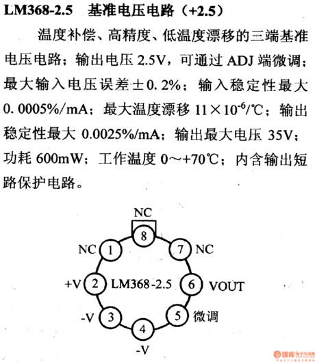
LM368-2.5 reference voltage circuit (+2.5V) This is a high-precision, low temperature drift and low-noise 3-terminal Vref circuit; its output voltage is 2.5V, which can be micro-adjusted by ADJ; its max input voltage fault is ±0.2%; the maximum input stability is 0.0005%/mA; its max temperature drift is 11*10-6/℃; its max output stability is 0.0025%/mA; it max output voltage is 35V; its power consumption is 600mW; its working temperature is 0~+70℃; it contains the output short circuit protection circuit.
(View)
View full Circuit Diagram | Comments | Reading(1147)
The regulator: DC-DC circuit, power supply monitor pin and its main features LM3999
Published:2011/8/30 2:22:00 Author:Seven | Keyword: DC-DC circuit, power supply, monitor pin
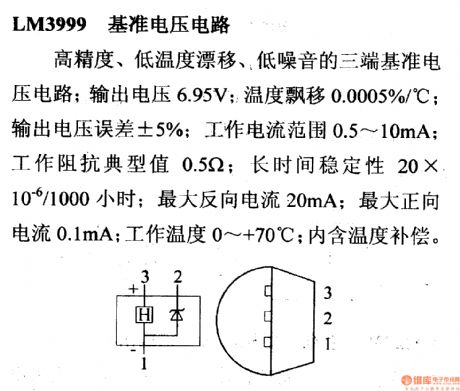
LM3999reference voltage circuitThis is a high-precision, low temperature drift and low-noise 3-terminal Vref circuit; its output voltage is 6.95V; temperature drift is 0.0005%/℃; output voltage fault is ±5%; working current range is 0.5~10mA; the typical value of its working impedance is 0.5Ω; the long-term time stability is 20*10-6/1000h; the maximum reversed current is 20mA; the maximum forward current is 0.1mA; its working temperature is 0~+70℃; it contains the temperature compensation.
(View)
View full Circuit Diagram | Comments | Reading(830)
The regulator: DC-DC circuit, power supply monitor pin and its main features LMC7660/7669
Published:2011/8/30 2:21:00 Author:Seven | Keyword: DC-DC circuit, power supply, monitor pin
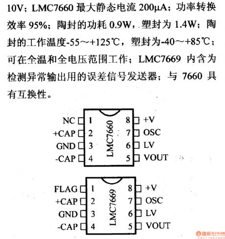
LMC7660/7669 CMOS voltage converterThis is a CMOS voltage converter generating the negative output whose voltage is equal to the positive output; it working voltage range is 1.5~10V; the max static current of LMC7660 is 200μA; the power converting efficiency is 95%; the power consumption of the pottery sealing is 0.9W; the working temperature is the pottery sealing is -55~+125℃, the plastic package is -40~+85%; it can work in the full temperature range and full voltage range.
(View)
View full Circuit Diagram | Comments | Reading(1245)
The regulator: DC-DC circuit, power supply monitor pin and its main features LM2930
Published:2011/8/30 2:24:00 Author:Seven | Keyword: DC-DC circuit, power supply, monitor pin
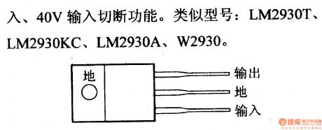
This is a low voltage gap 5-terminal regulator whose output voltage is stable; the output voltages are 5V and 8V; output current is 150mA; output voltage fault is ±2%; when the output current is 150mA, the minimum input-output voltage gap is low than 0.6V; the maximum input voltage is 26V; the working temperature is -40~85℃; it contains the current limitation, overheat protection, battery reversed polarity inserting, 40V input cutting-off and other functions. The approaching modes are LM2930T, LM2930KC, LM2930A and W2930.
(View)
View full Circuit Diagram | Comments | Reading(947)
The regulator: DC-DC circuit, power supply monitor pin and its main features LM2925
Published:2011/8/30 2:26:00 Author:Seven | Keyword: DC-DC circuit, power supply, monitor pin
LM2925-the 5V regulator (reset terminal) This is a low voltage gap 5-terminal regulator whose output voltage is stable; the output voltage is 5V; the maximum output current is 750mA; when the output is 500mA, the minimum input-output voltage gap is lower than 0.6V; when the output voltage is dropping, it is outputting a low but effective reset signal; the delaying time of the resetting signal output can be set by the external capacitors; the max input voltage is 26V; working temperature -40~+125℃; it contains functions of the current limitation, overheat protection, inverting inserting, 60V severing input and -50V transition state.
(View)
View full Circuit Diagram | Comments | Reading(809)
The regulator: DC-DC circuit, power supply monitor pin and its main features LM199A/299A/399A
Published:2011/8/30 2:28:00 Author:Seven | Keyword: DC-DC circuit, power supply, monitor pin
LM199A/299A/399A reference voltage circuit This a reference voltage circuit of high precision, low temperature drift and low noise; its output voltage is 6.95v; output voltage fault is ±2%(but LM399A); LM199A/299A temperature drift is 0.00005%/℃, and that of LM399A is 0.0001%/℃; its working current range is 0.5~10mA; its working impedance typical value is 0.5Ω; the typical value of long-term stability is 20*10-6/1000h; its inverting current is 10mA; the working temperature is LM199A is -55~+125℃, LM299A is -25~+85℃, LM399A is 0~+70℃.
(View)
View full Circuit Diagram | Comments | Reading(840)
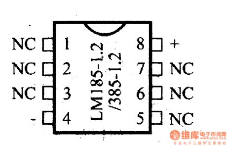
The regulator: DC-DC circuit, power supply monitor pin and main features LM185-2.5/285-2.5/385-2.5
Published:2011/8/30 2:29:00 Author:Seven | Keyword: DC-DC circuit, power supply, monitor pin
LM185-2.5/285-2.5/385-2.5 reference voltage circuit (+2.5V) This is a 2-terminal high-voltage circuit of high precision, low temperature drift and low noise; the output voltage is +2.5V; LM185-2.5/285-2.5 output voltage fault is ±1.5%, LM385-2.5 is ±3%; its working current range 20μA~20mA; temperature drift is 20*10-6/℃; the long-term time stability is 20*10-6/1000h; the maximum reversed current is 30mA; the maximum forward current is 10mA; LM185-2.5 working temperature is -55~+125℃, LM285-2.5 is -25~+85℃ and LM385-2.5 is 0~+70℃.
(View)
View full Circuit Diagram | Comments | Reading(742)
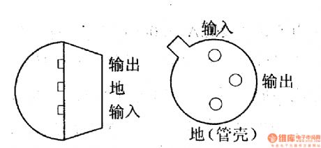
The regulator: DC-DC circuit, power supply monitor pin and its main features LM185/285/385
Published:2011/9/5 22:51:00 Author:Seven | Keyword: DC-DC circuit, power supply, monitor pin
LM185/285/385--the Vref circuitThis is a high-precision, low-temperature drift and low-noise circuit which allows no Vref diodes on its 2 terminals; the output voltage range is 1.24~5.30V; the output voltage fault is ±1%(B series); the working current range is 10μA~20mA; the typical value of working impedance is 1Ω; the max reversed current is 30mA; the max forward current is 10mA; the working temperature of LM185 is -55~+258℃, LM285 IS -55~+258℃ and LM385 is 0~+70℃.
(View)
View full Circuit Diagram | Comments | Reading(885)
The regulator: DC-DC circuit, power supply monitor pin and its main features LM140LA/340LA
Published:2011/8/24 21:52:00 Author:Seven | Keyword: DC-DC circuit, power supply, monitor pin
LM140LA/340LA--the 3-terminal stabilizer (forward output) This is a 3-terminal stabilizer with fixed output voltage; its output voltage can be 5V, 12v and 15V; its output current is 100mA; its input stability is 0.04%/V; its load stability is 0.01%/mA; its max input voltage is 35V; the working temperature of LM140LA is +55~+125℃ and that of LM340LA is 0~+70℃; it contains the current limitation, overheat cutoff and sate working area protection circuit; LM140LA is in metal package, LM340LA is in either metal or plastic package.
(View)
View full Circuit Diagram | Comments | Reading(928)
The regulator: DC-DC circuit, power supply monitor pin and its main features LM1578/2578/3578
Published:2011/9/5 22:52:00 Author:Seven | Keyword: DC-DC circuit, power supply, monitor pin
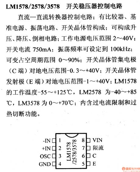
LM1578/2578/3578--the switch stabilizer control circuitThis is a DC-DC converter control circuit; it consists of the comparator, reference power supply, oscillating circuit and switch transistor; it can compose the booster, step-down and phase inverting circuit; the working power supply voltage range is 2~40V; the switch current is 750mA; the oscillating frequency can be set as 100kHz; the duty cycle period range is 0~90%; the voltage difference range between the electrode of the switch transistor (C terminal) and the earth is -0.3~+40V and that of the switch transistor emitter (E terminal) and the ground is -1~+40V.
(View)
View full Circuit Diagram | Comments | Reading(921)
The regulator DC-DC circuit, power supply monitor pin and its main features AN7800R, etc
Published:2011/8/24 21:49:00 Author:Seven | Keyword: regulator DC-DC circuit, power supply, monitor pin
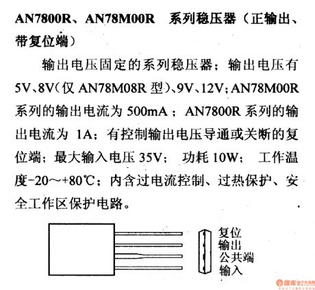
AN7800R and AN78M00R stabilizer (forward output with reset terminal) The output voltage solid stabilizer; the output voltages are 5V, 8V(AN78M08R only), 9V and 12V; AN7800R output current is 500mA; AN7800R output current is 1A; it has the reset terminal which controls output voltage conduction or breakdown; the maximum input voltage is 35V; power consumption is 10W; working temperature is -20~+80℃; it contains current control, over-heat protection, secure working area protection circuit. (View)
View full Circuit Diagram | Comments | Reading(768)
Lithium battery quick charger composed of LM3420-8.4
Published:2011/9/8 7:02:00 Author:Felicity | Keyword: Lithium battery, quick charger
This circuit adopted the specialized lithium battery charger LM3420-8.4 and it’s simple and have high performance and can charges two lithium batteries quickly. When the charging voltage reaches the rated value (with a single lithium battery it’s 4.2V), the charging current drops down to avoid permanent damage of lithium battery caused by overvoltage.
(View)
View full Circuit Diagram | Comments | Reading(2225)
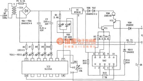
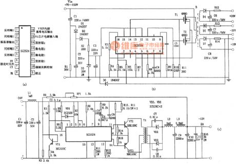
Application of PWM-based Switching-Regulator Power Controller SG3524
Published:2011/9/8 6:20:00 Author:Felicity | Keyword: PWM, Switching-Regulator, Power Controller
View full Circuit Diagram | Comments | Reading(8717)
Boosting Switching-Regulator Power Circuit Composed of 555
Published:2011/9/8 6:14:00 Author:Felicity | Keyword: Boosting, Switching-Regulator Power Circuit
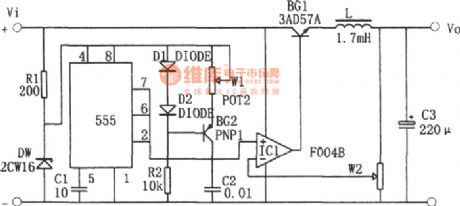
In the circuit, BG1 is the switch-adjusting transistor; operational amplifier IC1 composes the comparison amplifier; 555 time-base circuit is connected as astable multivibrator. The saw-wave voltage produced by the oscillator on C1 (Vmin=1/3Vz, Vmax=2/3Vz, the frequency determined by W1 and C1) is put onto the noninverting-terminal of the comparison amplifier IC1 and the sampling voltage is put onto the inverting-terminal of the comparison amplifier. (View)
View full Circuit Diagram | Comments | Reading(3310)
Lead accumulator charger circuit diagram
Published:2011/9/7 6:54:00 Author:Vicky | Keyword: Lead accumulator charger circuit
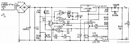
Lead accumulator charger circuit is shown in the above picture. The charger adopts constant voltage type charging. It controls the end of charging by the reduction of the charging current brought by the gradually adequate battery power. There is no need to worry about over-charging or lack of charging. When the power is on, the level of U1A inverting end , pin2, is always lower than the non-inverting input end, pin3. Therefore, pin 1 of U1A outputs high level, which makes Q1 saturate and conducted. It is as effective as the grounding of pin ADJ of U2, and the output of U2 is 1.2V with the charging end of 0.6A. It presents light load under such circumstance, and DS2 green luminous diodes is lighted. When the button S2 is pressed down, pin3 of U1A is grounded, pin2 is connected with the positive pole of the power via R1, then the U1A outputs low level, DS2 red luminous diode is lighted, and DS1 goes out. (View)
View full Circuit Diagram | Comments | Reading(2413)
Lead-acid cell over-charging protector circuit diagram
Published:2011/9/7 6:56:00 Author:Vicky | Keyword: lead-acid cell , over-charging protector circuit
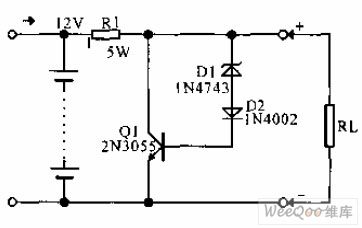
Lead-acid cell over-charging protector circuit is shown in the above picture. The protector can prevent middle size or large size lead-acid cell with capacity between 2 and 30 Ah from over-charging in the process of floating charging (the cell provides power for the load while being charged by trickle charge or solar panel). When it is not in the process of charging, Q1 cannot conduct the electricity due to the impedance of D1. When the charging voltage rises to about 14V, transistor Q1 (2N3055) is conducted, and splits the battery current to prevent the electrolyte from evaporating, which is beneficial for heat dissipation. Q1 should be assembled in a medium size heating panel. NTE143A can be also play the role of Q1. (View)
View full Circuit Diagram | Comments | Reading(2824)
Vehicle nickel-cadmium battery charger circuit diagram
Published:2011/9/7 6:58:00 Author:Vicky | Keyword: vehicle nickel-cadmium battery charger circuit
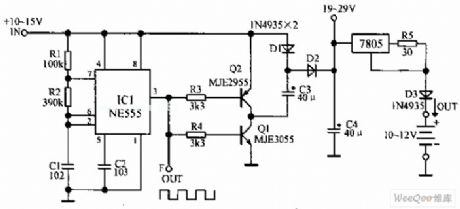
Vehicle nickel-cadmium battery charger circuit is shown in the above picture. It makes use of NE555 timer and two voltage multiplier circuits composed of power transistor so as to convert the voltage of vehicle battery from 12V to above 20V and then charge the 12V nickel-cadmium battery without changing the current. The voltage which has been multiplied sends the power current to three-end current stabilizer. NE555 are connected and form multi-vibrator, and the switch frequency is 1.4KHz. The charging current is set at 50mA, which can charge 10 pieces of 500mA·h nickel-cadmium batteries. (View)
View full Circuit Diagram | Comments | Reading(2388)
Circuit diagram of charger with diminishing pulse charging current exponentially
Published:2011/9/7 7:04:00 Author:Vicky | Keyword: charger, diminishing pulse charging current exponentially
Circuit diagram of charger with diminishing pulse charging current in accordance with index is shown in the above picture. A1 and A2 constitute controlled multi-vibrator. Set the threshold value at around 1.45V. Back electromotive force generated by the polarized electric fields of the battery during charging would directly influence the output state of A2. During the test, when conducting pulse charging to the current, the increasing and decreasing speed of the polarized electric field strength and the depth of electrochemical reaction inside the battery present exponentially changing. The circuit utilizes this discipline to regulate the frequency and pulse brand of the pulse charging current and to realize the goal of controlling.
(View)
View full Circuit Diagram | Comments | Reading(2301)
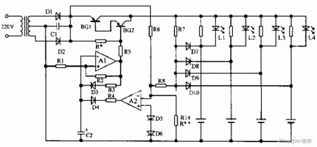
Circuit diagram of prolonging the lifetime of nickel-cadmium battery
Published:2011/9/7 7:00:00 Author:Vicky | Keyword: nickel-cadmium battery, prolonging the lifetime
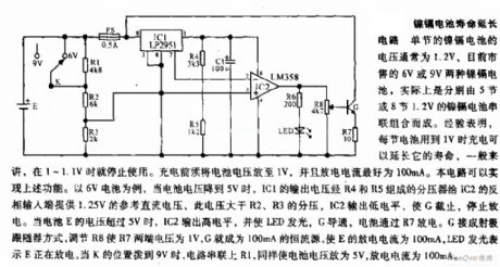
Circuit diagram of prolonging the lifetime of nickel-cadmium
Generally, the voltage of a single nickel-cadmium battery is 1.2V. 6V or 9v nickel-cadmium battery sold in the market now is in fact made of 5 or 8 nickel-cadmium battery of 1.2V in serial. Experience suggests that the lifetime of a battery can be prolonged when it was charged with still 1V left. Generally speaking, a battery should not be used when there is 1~1.1V left. The battery voltage must be reduced to 1V before charging, and the best discharging current is 100mA. The circuit in the picture can realize the above function. Take 6V battery as an example. When the battery voltage reduces to 5V, output voltage of IC1 provides the reference DC voltage of 1.25V for inverting input end of IC2 by voltage divider composed by R4 and R5. The reference voltage is higher than the divided voltage of R2 and R3. IC2 outputs low level which stops G, and the discharging stops. When the voltage of battery E is higher than 5V, IC3 outputs high level, and makes LED lighted, G conducted, and battery discharges via R7. (View)
View full Circuit Diagram | Comments | Reading(1311)
Pulse express charger circuit diagram
Published:2011/9/7 7:02:00 Author:Vicky | Keyword: pulse, express charger
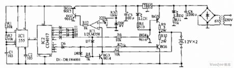
Pulse express charger circuit is shown in the above picture. This nickel-cadmium battery charger can reduce undesirable polarization and prolong the lifetime of battery. In the circuit, 555 are connected and form astable vibrator, which is uses as clock with frequency of about 500Hz. The astable vibrator controls decimal counter CD4017 to output square wave pulse. It then conducts high-current pulse charging and discharging with a proportion of 5:1 to the nickel-cadmium battery after amplified by power tube. There are intermittent pauses during the charging and discharging. During the pauses,check the voltage of the battery by the calculating amplifier. When the battery is full charged, the circuit automatically stops charging. (View)
View full Circuit Diagram | Comments | Reading(3491)
| Pages:60/291 At 204142434445464748495051525354555657585960Under 20 |
Circuit Categories
power supply circuit
Amplifier Circuit
Basic Circuit
LED and Light Circuit
Sensor Circuit
Signal Processing
Electrical Equipment Circuit
Control Circuit
Remote Control Circuit
A/D-D/A Converter Circuit
Audio Circuit
Measuring and Test Circuit
Communication Circuit
Computer-Related Circuit
555 Circuit
Automotive Circuit
Repairing Circuit