
power supply circuit
Index 50
The power supply circuit diagram of CASPER CM-1489 dual frequency monochrome display
Published:2011/11/10 2:10:00 Author:May | Keyword: power supply, CASPER, dual frequency, monochrome display
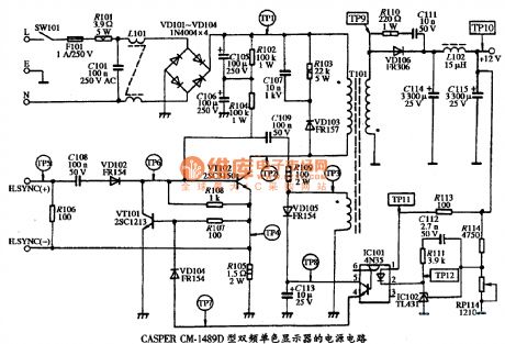
View full Circuit Diagram | Comments | Reading(1456)
The power supply circuit diagram of IBM 5153-002 color display
Published:2011/11/10 2:11:00 Author:May | Keyword: power supply, color display, IBM
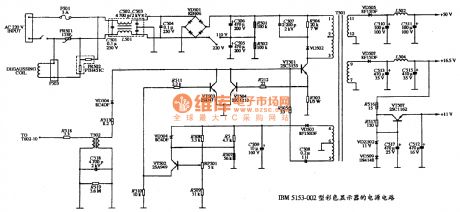
View full Circuit Diagram | Comments | Reading(3572)
The power supply circuit diagram of SUPERSYNC MD-14III, SUPERSYNC PWB-1509 type color display
Published:2011/11/10 2:14:00 Author:May | Keyword: power supply, color display, SUPERSYNC
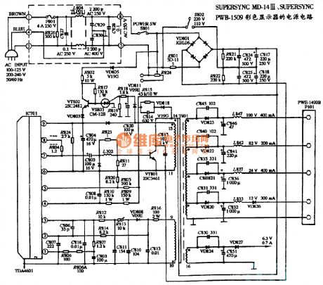
View full Circuit Diagram | Comments | Reading(1042)
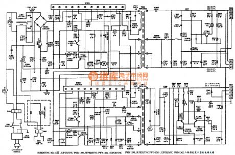
The power supply circuit diagram of three kinds color display
Published:2011/11/10 2:13:00 Author:May | Keyword: power supply, color display, SUPERSYNC
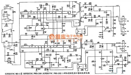
The power supply circuit diagram of SUPERSYNC MD-11III, SUPERSYNC PWB-1369, SUPERSYNC PWB-1505 color display (View)
View full Circuit Diagram | Comments | Reading(993)
The power supply circuit diagram of six color displays
Published:2011/11/10 2:20:00 Author:May | Keyword: power supply, color display, SUPERSYNC
The power supply circuit diagram of SUPERSYNC MD-10III, SUPERYNC PWB-1290, SUPERSYNC PWB1291, SUPERSYNC PWB-1293, SUPERSYNC PWB-1361, SUPERSYNC PWB-1362 color displays
(View)
View full Circuit Diagram | Comments | Reading(1267)
Blocking AC power supply with TDA4600
Published:2011/11/23 2:04:00 Author:May | Keyword: Blocking AC, power supply
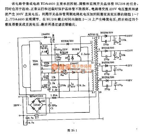
Integrated circuit TDA4600 in this circuit mainly has the task of controlling, adjusting and overseeing switching BU208. Meanwhile it isalso used to protect transistor from damaging in starting, normal operating and over load. AC 220V voltage is rectified and filtered by the circuit. And then it can generate 300V DC voltage. It can periodically add this voltage to winding 1~7 of blocking AC transformer by utilizing switching transistor. And TDA4600 is achieved adjusting. In the period of BU208 cut off, it can generate 3 peak value voltage on winding 2~16, then it is rectified to DC voltage by four rectifiers, finally, it is output by filter. (View)
View full Circuit Diagram | Comments | Reading(2003)
APM-81 elevator door driver and mun circuit
Published:2011/8/26 3:50:00 Author:Jessie | Keyword: elevator door driver , mun
View full Circuit Diagram | Comments | Reading(1308)
Reference voltage source using BJT
Published:2011/11/23 2:21:00 Author:May | Keyword: Reference voltage source using BJT

This circuit adopts voltage regulator tube D1, transistor T and resistor R1, R2 to make up constant-current source. It can supply for parallel circuit composed of reference diode D2 and load resistor RL (here is 68kΩ). Its current is about 7.6mA. Because the current on D1 is much higher than base-emitter current of transistor and the current on D1 is designed to be very high (5mA), the change of emitter current and reference diode current caused by the dispersion of transistor data and input current is very small.
(View)
View full Circuit Diagram | Comments | Reading(2312)
Constant current source using operational amplifier TAA861
Published:2011/12/5 0:54:00 Author:May | Keyword: Constant current source, operational amplifier
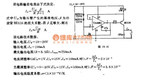
The output current of this circuit is determined by the following formula:IA=(Uref β)/R β+1 AIn the formula: Uref is reference voltage generated by voltage regulator tube, β is magnification coefficient of power tube. If β is big enough, IA≈Uref/R AThe technical data of this circuit:input voltage: UE=10~20Voutput current: IA=100mAlargest output current (R=805Ω): IAmax≈750mAcurrent adjustable rate (when △UE=1V, UE=15V, IA=100mA): F= △IA/IA=2×10-4load adjustable rate (when Ua=0~10V, UE=15V, IA=100mA): F=△IA/IA=1.6×10-3output current temperature factor: α<5×10⁻⁴V/K (View)
View full Circuit Diagram | Comments | Reading(2081)
30W micro switch regulated power supply composed of TOP224Y
Published:2011/12/5 1:25:00 Author:May | Keyword: 30W, micro switch, regulated power supply
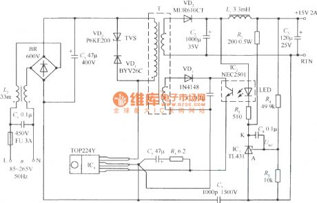
Here we introduce a kind of 30W micro switch regulated power supply composed of TOP224Y, its circuit is shown in the diagram. Its feature is using TL431 to replace regulation tube VDz2 in the sampling circuit. That is, it can reach the technical target of micro switch power supply by using high stability band gap reference voltage Uref to replace normal zener diode. The excellent characteristic is concentrated reflecting on, when AC input voltage u changes from 85V to 265V, Sv=±0.2%; when load current changes from 10% (0.2A) to 100% (2A), S1=±0.2%. It can compare with linearity integrated power supply.
Electric isolation outside error amplifier consists of TIA31(IC3) and optical coupler NEC2501(IC2). When it is conncted with internal error amplifier, it can greatly improve regulation performance by precision adjusting the control end of TOP224Y(IC1). It can get sampling voltage after +15V regulation output dividing by R4 and R5. Compared with TL431's internal 2.5V reference voltage, it can adjust control end current Ic by changing potential of K end to control LED's current. R4 and C8 also can determine the frequency property of outside error amplifier.
(View)
View full Circuit Diagram | Comments | Reading(7273)
Forward conversion type switching stabilized voltage supply isolating by photocoupler
Published:2011/11/22 1:28:00 Author:May | Keyword: Forward conversion, switching, stabilized voltage supply, photocoupler
The diagram shows forward conversion switching stabilized voltage supply isolated by photo-coupler. VT1 is switching tube; VT2 and the photistor of photo-coupler VT3 make up compound variable resistance tube; VT4 and VT5 make up compound error amplifier. N2 is the secondary winding of high transformer T for DC outputting and sampling. N3 is self-oscillation positive feedback coil. In this circuit, DC voltage output end connects with sampling circuit of error amplifier, but thesignal output by amplifier is not connecting to the circuit, thereby it achieves the electrical isolation of sampling circuit for error amplifier and switching tube.
When output voltage increases, emitter current of compound error amplifier VT4 and VT5 increases. This current passes the LED in photo-coupler to make its illumination become larger. (View)
View full Circuit Diagram | Comments | Reading(1046)
Matsushita L12H power supply
Published:2011/11/22 1:04:00 Author:May | Keyword: Matsushita, power supply
TV using Matsushita L12H power supply includes: Matsushita TC-230H, TC-2030DHN, TC-830D, TC-840D, etc.
Oscillation circuit
One way of the 300V DC voltage on the C836 is added to the internal switch's C pole of IC801 pin 1 by the P1, P2 windings of T801, then it is added to the B pole of the IC801's pin 2 internal tube by the R803, then the switch tube begins to turn on, E polar current is out from IC801's pin (4). T801's P1, P1 winding current increases to generate induced voltage and couple to the F2, F3 windings, then F2, F3's induced voltage polarity is that the F3 is negative and F2 is positive, the voltage is added to the IC801 (2 ), ( 4 ) feet through C806, R804, so that the switch current is further increased, and the strong positive feedback make the switch be quickly saturated . (View)
View full Circuit Diagram | Comments | Reading(1315)
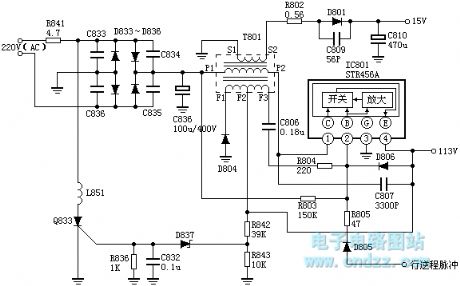
Matsushita L15 power supply
Published:2011/12/5 1:21:00 Author:May | Keyword: Matsushita, power supply
The model number of TV which using Matsushita L15 power supply have: TC2171, TC2173, TC2185, TC2186, TC-D21, TC-D25, etc. Main switch power supply consists of STR50213 which belongs to series stabilized voltage supply.
Oscillation circuit
Q834 is 113V overvoltage protection circuit. When 113V is normal, Q834 is cut off. If 113V is too high, Q834 is turned on. If 113V is in short circuit, the oscillation stop.
APS and remote control shutdown circuit
When the TV is normally starting, CPU’s pin 6 outputs high level. It will make Q814 turn on. At this time, Q810, Q811, Q812, Q813 are all cut off. And APS is not working. (View)
View full Circuit Diagram | Comments | Reading(1847)
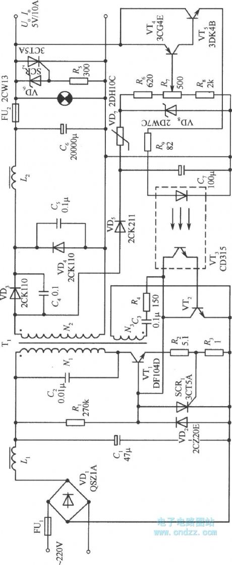
Separate excitation switching regulated power supply 2
Published:2011/12/5 1:19:00 Author:May | Keyword: Separate excitation, switching regulated power supply

The diagram is theseparate excitation switching regulated power supply circuit which uses single-junction transistor as pulse generator. VDl ~ VD4 and C1form rectifier filter circuit, it can change 220V AC mains voltage into 300V DC voltage. Pulse generator consists of single junction transistor VT1, resistors R3, R4, R5, potentiometer Rp and capacitor C3. And changing the resistance of the potentiometer Rp can change the pulse frequency. C4 is coupling capacitor of output pulse. R1 and R2 can divide 300V DC voltage and send 20~30V working voltage of single junction transistor VT1. VT2 is inverting amplifier tube. It can invert andamplify positive polarity pulse output by pulse generatorand send negative polarity pulse to switching tube VT2, it can make itself cut off when VT1 outputs positive polarity pulse.
VT3, R7, C5 make up protection circuit of switching tube VT4. (View)
View full Circuit Diagram | Comments | Reading(1853)
Push pull type switching regulated power supply principle diagram
Published:2011/11/21 21:15:00 Author:May | Keyword: Push pull type, switching regulated power supply
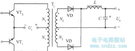
Push-pull converter circuit belongs to double-ended type conversion circuit. Its high-frequency transformer works atboth sides of the hysteresis loop. The typical circuit is shown as the chart. Switching transistors VT1, VT2 are alternately turned on and off after inspiring by base driving circuit, the input DC voltage Ui is converted into high frequency square wave AC voltage. When VTl is turned on, Ui is added to the primary winding N1 of the transformer T1 by VT1. When the base incentive disappears, VTl, VT2 tubes are closed. The collector voltage is input voltage Ui. Next half cycle, VT2 is turned on, VTl is ended, VT1 can add two times input voltage, after the two tubes cut off, and the next cycle is started again. The main disadvantage of push-pull circuit isthat switching transistor voltage should reach 2 times of input power. To take 220 ± 10% V grid voltage for an example of peak voltage, the maximum steady state cutoff voltage is 680V. (View)
View full Circuit Diagram | Comments | Reading(1863)
Practical circuit of push-pull converter type switching regulated power supply
Published:2011/11/21 21:20:00 Author:May | Keyword: push-pull converter type, switching regulated power supply
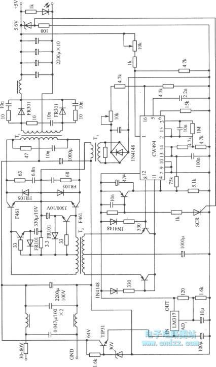
The diagram shows a practical circuit of push-pull converter type switching regulated power supply. CW494 is double-ended converter modulator integrated circuit which includes error amplifier, voltage reference, clock oscillator, pulse width modulator and other circuits. Transformer T1 is high-frequency transformer which can transfer energy to the load. T2 is incentive promotion transformer. It can transmit two strings of pulse modulator outputted by CW494 pulse modulator to drive and switching tube base of push pull circuit after it enlarged through incentives promote transistor. Winding transformer T3 is the sampling pulse of AC voltage on the transformer and rectified through by the sample sent to the pulse modulation circuit resistance CW494 16 feet, as the error amplifier inverting input.
The selection of power switching power transistor is fast series F461. In the place where the voltage is feedback, input and output are directly connected. If the input and output need to be isolated, the optocoupler can be used. (View)
View full Circuit Diagram | Comments | Reading(1819)
Output sampling winding isolated switching power supply
Published:2011/11/22 0:07:00 Author:May | Keyword: Switching power supply, output sampling, winding isolated
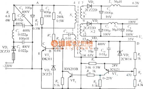
The diagram shows the output sampling winding isolated switching power supply . In diagram, T is high frequency transformer; N2 is self-oscillation positive feedback winding; N3 is the error amplifier , and VTSis thewinding to provide sampling signal; N4, N5are DC output windings. DC output and the power gridare isolated from each other, because N3, N4, N5 are isolated from each other.
The power supply has two sets output of 6.3V and 100V DC. 35V voltage is used in error amplifier.
When output voltage is increasing, the sampling resistor’s voltage UD is increasing, error amplifier VT3’s collector current is increasing. Positive partial voltage offered to variable resistance tube VT2 by voltage drop of resistor R8 generated by the current is increasing, so that the collector current of VT2 is increasing.
The voltage dropping Ucd2 is reduced to be equivalent to the shunt resistor between base of switching tube VT1 and ground. (View)
View full Circuit Diagram | Comments | Reading(3030)
Dual output switching regulated power supply
Published:2011/11/22 0:47:00 Author:May | Keyword: Dual output, switching, regulated power supply
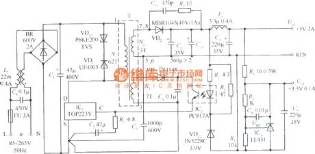
The circuit diagram of 15W switching regulated power supply with +5V (3A) main output and +3.3V (0.1A) alternative output is shown in the following diagram. This power supply adopts one piece of TOP223Y type single chip switching power supply with TO-220 packaging. Its maximum output power is 30W. It can use the power supplyfor printer and monitor. If the main power supply is +3.3V, it can be used for the switching power supply of notebook. The input voltage range of this power supply is 85~265V. The voltage regulation factor is ±0.7%, load regulation factor is +1.1%, power supply efficiency η>70%.
The features of this power supply is shown in the following: (1) it can output +5V, +3.3V two loads isolation stable voltage at the same time; (2)It can further improve the stability of _5V and +3.3V output voltage to add one piece adjustable precision parallel voltage regulator IC3 (TL431) ; (3)it adds RC absorb circuit composed of C11, R7 to eliminate high frequency self-oscillation and decrease radio frequency interference (RFI). (View)
View full Circuit Diagram | Comments | Reading(3422)
Boost chopping type switching stabilized voltage supply principle diagram
Published:2011/11/22 0:44:00 Author:May | Keyword: Boost, chopping type, switching stabilized voltage supply
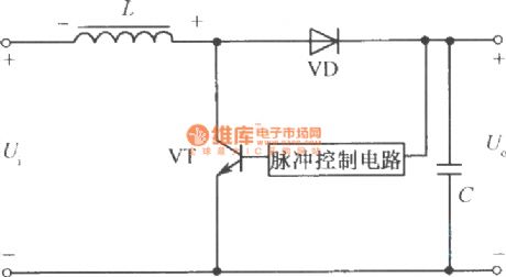
The diagram is boost chopping type switching stabilized voltage supply principle diagram. When switching component is controlledto besaturation conduction, the current passing inductor to make it store energy. When switching component VT is controlled and in the cut-off state, the energy stored in inductor still offers to load through diode VD, meanwhile it is charging to capacitor C. When load voltage is dropping down, the capacitor is discharging again. At this time, it can get stable voltage which is higher than input voltage. It is also called parallel switching stabilized voltage supply, because switching component VT and load resistor RL is parallel. (View)
View full Circuit Diagram | Comments | Reading(819)
Practical circuit of zero current switching soft switching stabilized voltage supply
Published:2011/11/21 20:50:00 Author:May | Keyword: zero current switching, soft switching, stabilized voltage supply
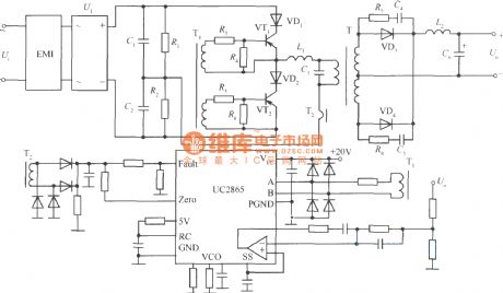
The diagram is a practical circuit ofzero current switchingsoft switching stabilized voltage supply. Its input is single phase alternating current. Its output is direct current. The main switching tube adopts MOSFET. Power switching circuit adopts half bridge circuit. Integrated control chip uses UC2865. Its power switching mode adopts zero current switching circuit.
(View)
View full Circuit Diagram | Comments | Reading(1715)
| Pages:50/291 At 204142434445464748495051525354555657585960Under 20 |
Circuit Categories
power supply circuit
Amplifier Circuit
Basic Circuit
LED and Light Circuit
Sensor Circuit
Signal Processing
Electrical Equipment Circuit
Control Circuit
Remote Control Circuit
A/D-D/A Converter Circuit
Audio Circuit
Measuring and Test Circuit
Communication Circuit
Computer-Related Circuit
555 Circuit
Automotive Circuit
Repairing Circuit