
power supply circuit
Index 58
Regulator DC-DC Circuit and MAX663 CMOS Regulator
Published:2011/9/13 2:35:00 Author:Zoey | Keyword: Regulator, DC-DC Circuit,
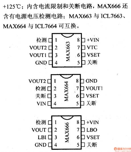
MAX663/666 refers to CMOS positive output regulator, while MAX664 refers to the negative one. If VSET is connected to the ground, output voltage of MAX663/666 will be 5V, and MAX666 will be -5V. If VSET is connected to external resistance, output voltage range of MAX663/666 will be 1.3~16V, and MAX664 will be -1.3~-16V. The output current is 40mA, static current is 12µA. Input voltage range of MAX663/666 is 2~16.5V, MAX664 is -2~-16.5V. Working temperature range of MAX663C/664C/666C is 0~+70℃, MAX663E/664E/666E -40~+85℃, MAX663M/664M/666M -55~+125℃. This regulator has circuits for current-restriction and power-off. MAX666 has a detection circuit for voltage of power supply. (View)
View full Circuit Diagram | Comments | Reading(928)
Regulator DC-DC Circuit and Pin of Power Supply Monitor and its Main Features TA78L00P Regulator
Published:2011/9/13 0:14:00 Author:Zoey | Keyword: Regulator, DC-DC Circuit, Pin of Power Supply Monitor
TA78LOOP series Three-terminal Regulator
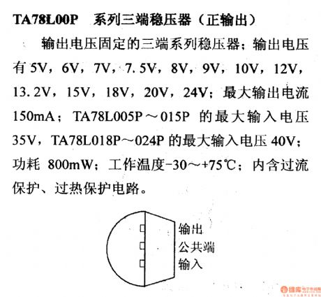
Three-terminal regulators can output fixed voltage, the voltage can be 5V, 6V, 7V, 7.5V, 8V, 9V, 10V, 12V, 13.2V, 15V, 18V, 20V, 24V. The maximum current output is 150mA, the maximum voltage of TA78L005P~015p is 35V, and TA78L018P~024P is 40V. The power is 800mW and the working temperature is between -30 to +75 ℃. This circuit itself has interior overcurrent and overtemperature proof devices. (View)
View full Circuit Diagram | Comments | Reading(897)
Regulator DC-DC Circuit and Pin of Power Supply Monitor and its Main Features-MAX630
Published:2011/9/13 3:00:00 Author:Zoey | Keyword: Regulator, DC-DC Circuit, COMS, Boost converter
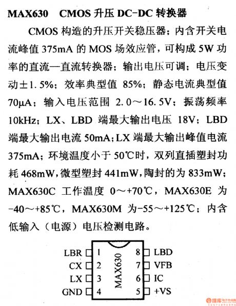
MAX638 CMOS DC-DC boost converter is a switched regulator, it has a interior MOS FET that has a peak of 375mA, this FET can constitute a 5-W DC-DC converter. Its voltage output is adjustable and input volage range is 2.0~16.5V. For this converter, typical efficiency is 85%, voltage variation ±1.5%, typical static current 70µA, oscillation frequency 10kHz. Maximum ouput voltage of LX and LBO terminal is 18V, peak of output current of LX is 375mA, LBO 50mA. If room temperature drops to below 50℃, power of DIP platic encapsulation will be 468mW, micro platic encapsulation will be 441mA, and ceramic encapsulation 833mW. Working temperature range of MAX630C is 0~+70℃, MAX630E -40~+85℃, MAX630M -55~+125℃. This converter has an interior circuit for input voltage-detection.
(View)
View full Circuit Diagram | Comments | Reading(740)
Regulator DC-DC Circuit and Pin of Power Supply Monitor and its Main Features-MAX631
Published:2011/9/13 2:59:00 Author:Zoey | Keyword: Regulator, DC-DC Circuit, CMOS, Boost Converter
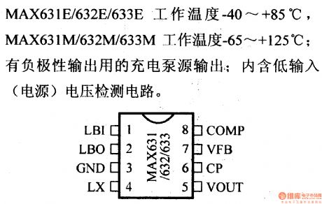
MAX631/632/633 CMOS DC-DC boost converter is a switched regulator, it has a interior MOS FET that has a peak of 325mA, this FET can constitute a DC-DC converter with a fixed output. Therein, MAX 631 5V, MAX632 12Vand MAX633 15V.For this converter, typical efficiency is 80%, typical working current 135µA, output voltage error 5% and 10%, oscillation frequency 45kHz. Maximum voltage of VOUT, LX and LBO terminal is 18V, peak of output current of LX is 325mA, LBO 50mA. If room temperature drops to below 50℃, power of DIP platic encapsulation will be 625mW, micro platic encapsulation will be 450mA, and ceramic encapsulation 800mW. Working temperature range of MAX631C/632C/633C is 0~+70℃, MAX631E/632E/633E -40~+85℃, MAX631M/632M/633M -65~+125℃. This converter has an interior circuit for low input voltage-detection and an output pump for spare negative ouput.
(View)
View full Circuit Diagram | Comments | Reading(911)
Regulator DC-DC Circuit and Pin of Power Supply Monitor and its Main Features- MAX635/636/637
Published:2011/9/13 2:54:00 Author:Zoey | Keyword: Regulator, DC-DC Circuit, COMS, Boost Converter, Inverted Output
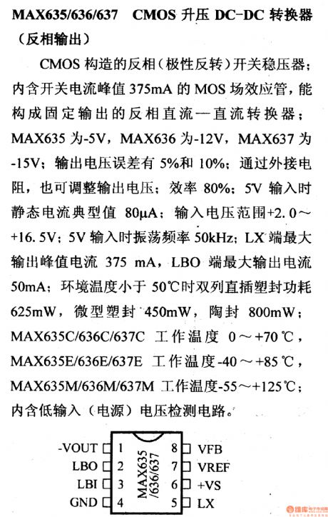
MAX635/636/637 CMOS DC-DC boost converter is a switched inverted regulator, it has a interior MOS FET that has a peak of 375mA, this FET can constitute an inverted DC-DC converter with a fixed output. Therein, MAX 635 -5V, MAX636 -12V and MAX633 -15V.For this converter, typical efficiency is 80%. When the input voltage reaches 5V, typical static current will be 85µA, oscillation frequency 45kHz and range of input voltage +2.0V~+16.5V. Peak of output current of LX terminal is 325mA, LBO 50mA. If room temperature drops to below 50℃, power of DIP platic encapsulation will be 625mW, micro platic encapsulation will be 450mA, and ceramic encapsulation 800mW. Working temperature range of MAX635C/636C/637C is 0~+70℃, MAX635E/636E/637E -40~+85℃, MAX635M/636M/637M -55~+125℃. This converter has an interior circuit for low input voltage-detection
(View)
View full Circuit Diagram | Comments | Reading(829)
Regulator DC-DC Circuit and Pin of Power Supply Monitor and its Main Features-MAX639
Published:2011/9/13 2:43:00 Author:Zoey | Keyword: Regulator, DC-DC Circuit, Pin, Adjustable Buck regualtor
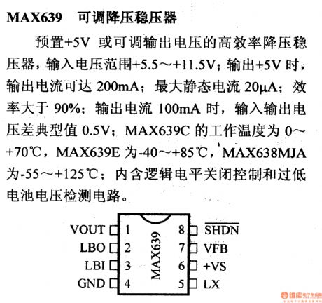
Output voltage (adjustable) range of MAX639 buck regulator is +5.5V~+11.5V. When output voltage reaches +5V, the output current can be 200mA, and maximum static current can be 20µA, efficiency will exceed 90%. If the current is 100mA, typical value of margin between input and ourput voltage will be 0.5V. Working temperature range of MAX639C is 0~+70℃, MAX639E -40~+85℃, MAX638MJA -55~+125℃. This converter has an interior logic level-close controller and a circuit for low voltage detection of the cells. (View)
View full Circuit Diagram | Comments | Reading(791)
Regulator DC-DC Circuit and Pin of Power Supply Monitor and its Main Features-MAX624
Published:2011/9/13 3:01:00 Author:Zoey | Keyword: Regulator, DC-DC Circuit, Binary output Converter
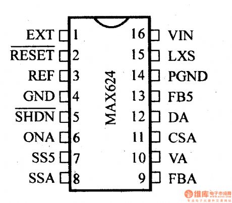
Switching frequency of MAX624 binary output DC-DC converter is 1MHz, working voltage range is 3.0~5.0V, static working current is 0.5mA, power-off current is 40µA. When the working turns to 5V, efficiency of SMPS will be 85%, input voltage 3V~5.5V, output voltage 5V±4%, output current 200mA, auxiliary output voltage 12V±2%. (View)
View full Circuit Diagram | Comments | Reading(859)
Regulator DC-DC Circuit and Pin of Power Supply Monitor and its Main Features-MAX638
Published:2011/9/13 2:45:00 Author:Zoey | Keyword: Regulator, DC-DC Circuit, CMOS, Buck Converter
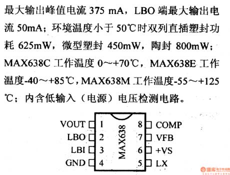
MAX638 CMOS DC-DC buck converter is a switched regulator, it has a interior MOS FET that has a peak of 375mA, this FET can constitute a DC-DC converter. Its voltage output can be adjusted by external resistance. For this converter, typical efficiency is 85%, typical static current 135µA, oscillation frequency 65kHz. Maximum voltage of LX terminal and LBO terminal is 18V, peak of output current of LX is 375mA, LBO 50mA. If room temperature drops to below 50℃, power of DIP platic encapsulation will be 625mW, micro platic encapsulation will be 450mA, and ceramic encapsulation 800mW. Working temperature range of MAX638 is 0~+70℃, MAX638 -40~+85℃, MAX638M -55~+125℃. This converter has an interior circuit for input voltage-detection. (View)
View full Circuit Diagram | Comments | Reading(822)
RegulatorDC-DC Circuit and Pin of Power Supply Monitor and its Main Features
Published:2011/9/13 0:22:00 Author:Zoey | Keyword: Regulator, DC-DC Circuit, Pin of Power Supply Monitor, Main Features
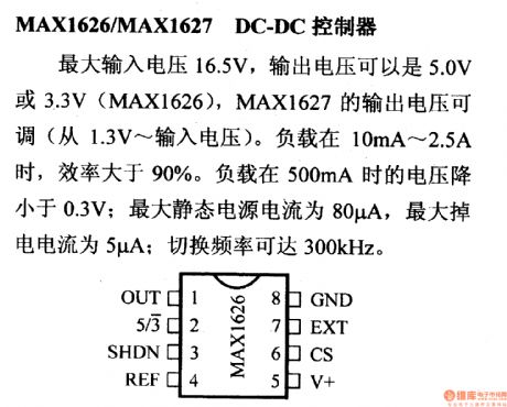
The maximum input voltage of MAX1626/MAX1627 DC-DC controller is 16.5V, output voltage of MAX1626 can be 5.0V or 3.3V,while output voltage of MAX1627 can be adjusted from 1.3V to itsinput voltage. If the load is between 10mA to 2.5A, efficiency will exceed 90%. Voltage will descend to below 0.3V when the load ranges from 10mA to 2.5A. The maximum static current of the power supply is 80µA, the maximum power-off current is 5µA. The Switched frequency can be as large as 300kHz. (View)
View full Circuit Diagram | Comments | Reading(956)
Regulator DC-DC Circuit and Pin of Power Supply Monitor and its Main Features-MAX608
Published:2011/9/13 3:02:00 Author:Zoey | Keyword: Regulator, DC-DC Circuit, Power supply, High-efficiency Controller
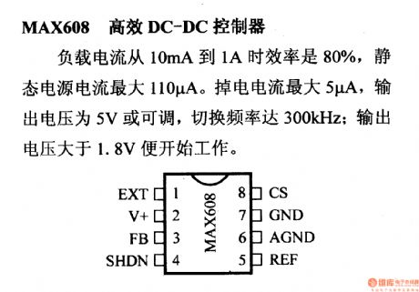
Ifload current of MAX608 high-efficiency DC-DC controller ranges from 10mA to 1A, its efficiency will be 80% and static current of power supply will be 110µA. For this controller, the maximum power-off current is 5µA, output voltage is 5V or adjustable, the switching frequency can reach 300kHz. This controller will begin towork as soon as voltage exceed 1.8V.
(View)
View full Circuit Diagram | Comments | Reading(855)
Regulator DC-DC Circuit and Pin of Power Supply Monitor and its Main Features-MAX606/MAX607
Published:2011/9/13 3:02:00 Author:Zoey | Keyword: Regulator, DC-DC Circuit, Pin of Power Supply Monitor, step-up converter
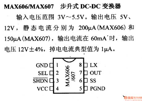
The input voltage range of MAX606/MAX607 step-up converter is 3V~5.5V. Its output voltage is 5V or 12V. Static current of MAX606 is 200µA and MAX607 is 150µA. If output current reaches 60mA, output voltage will turn to be 12V±4%. Typical value of its power-off current is 1µA. (View)
View full Circuit Diagram | Comments | Reading(786)
Regulator DC-DC Circuit and Pin of Power Supply Monitor and its Main Features-MAX603/MAX604
Published:2011/9/13 2:49:00 Author:Zoey | Keyword: Regulator, DC-DC Circuit, Pin of Power Supply Monitor, Linear Regulator
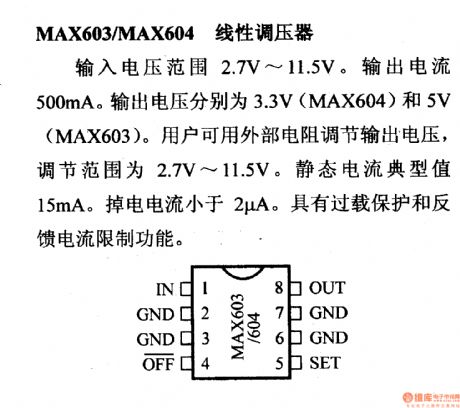
The input voltage range of MAX603/MAX604 linear regulator is 2.7V~11.5V. Its output current is 500mA, output voltage of MAX604 is 3.3V, MAX603 5V. External resistance regulator can be used to adjust output voltage, the adjusting range is 2.7V~11.5V. Typical value of static current is 15mA, power-off current is 2µA.This regulator has such functions as overload-proof and restrictions on feedback current. (View)
View full Circuit Diagram | Comments | Reading(1526)
Regulator DC-DC Circuit and Pin of Power Supply Monitor and its Main Features-MAX736/737 Regulator
Published:2011/9/13 2:32:00 Author:Zoey | Keyword: Regulator, DC-DC Circuit, Pin
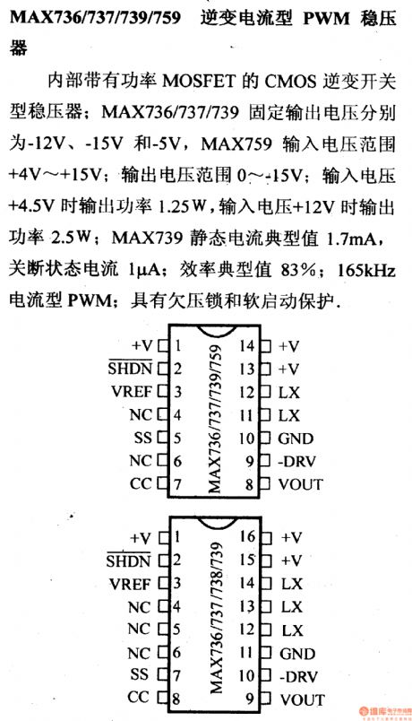
The MAX736/737/739/759 PWM regulator refers to the CMOS countercurrent switched regulator that has an interior power MOSFET. Fixed output voltage of MAX736/737/739 are -12V,-15V and -5V respectively. Input voltage range of MAX759 is +4V~+15V, output voltage range is 0~+15V. If the input voltage is +4.5V, output power will be 1.25W, and when it ascends to +12V, output power will be 2.5W. Typical value of static current of MAX739 is 1.7mA. In a power-off state, the current is 1μA. Typical value of efficiency is 83%. 156-kHz current PWM has an undervoltage lock and a soft-start protection device.
(View)
View full Circuit Diagram | Comments | Reading(832)
Regulator DC-DC Circuit and Pin of Power Supply Monitor and -MAX672/673 Reference Voltage Circuit
Published:2011/9/13 2:34:00 Author:Zoey | Keyword: Regulator, DC-DC Circuit, Reference Voltage Circuit
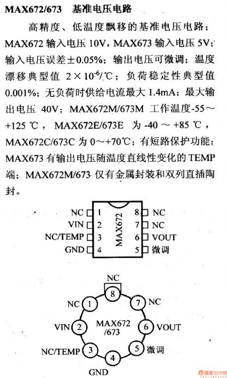
MAX672/673 reference voltage circuit (+10V) has thefeatures such as high accuracy, low temperature drift. Input voltage of MAX672 is 10V, of MAX673 is 5V. For this circuit, the input voltage error ±0.05% and output voltage can be adjusted slightly. The typical temperature drift is 2×10⁻⁶/℃, typical value of stable load is 0.001%, and no-load maximum input current is 1.4mA. The maximum output voltage is 40V. Working temperature of MAX672M/673M is -55~+125℃, MAX672E/673E -40~+85℃,. MAX672C/673C 0~+70℃.. The circuit itself has an interior short-circuit-proof circuit. Output voltage of TEMP terminal of MAX673 linearly changes with temperature. For MAX672M/673, only metal encapsulation and DIP ceramic encapsulation are available. (View)
View full Circuit Diagram | Comments | Reading(814)
Regulator DC-DC Circuit and Pin of Power Supply Monitor and its Main Features-MAX864 Converter
Published:2011/9/13 2:18:00 Author:Zoey | Keyword: Regulator, DC-DC Circuit, Pin, Converter
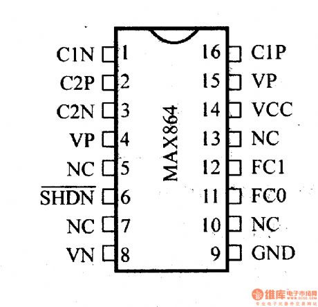
MAX864 dual-output voltage pump charging converter can input 1.5V~6.2V voltage. When input voltage ascends to 3V, the converter will get ±6.0-V output voltage. And when it ascends to 5.0V, it will get ±10-V output voltage. The output current is 10mA, and the switching frequency can be 5kHz, 30kHz, 100kHz or 200kHz. Its static current is 200µA.This converter only needs four 1-µF external capacitors. (View)
View full Circuit Diagram | Comments | Reading(857)
Regulator DC-DC Circuit and Pin of Power Supply Monitor and its Main Features-MAX865 Converter
Published:2011/9/13 2:12:00 Author:Zoey | Keyword: Regulator, DC-DC Circuit, Pin of Power Supply Monitor, Converter
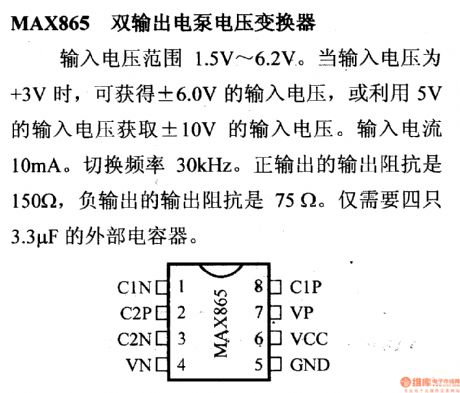
MAX865 dual-output voltage pump converter can input 1.5V~6.2V voltage. When the input voltage ascends to +3V, the converter will get ±6.0-V input voltage, or it will get ±10-V input voltage by using 5-V input voltage. The input current is 10mA, and the switching frequency is 30kHz. Impedance of positive output is 150Ω, while impedance of negative output is 75Ω. This converter only needs four 3.3-µF external capacitors.
(View)
View full Circuit Diagram | Comments | Reading(817)
Regulator DC-DC Circuit and Pin of Power Supply Monitor and Reverse DC-DC Converter
Published:2011/9/13 2:22:00 Author:Zoey | Keyword: Regulator, DC-DC Circuit, Pin of Power Supply Monitor, RP
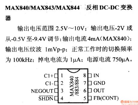
Voltage output of MAX840/MAX843/MAX844 RP DC-DC converters ranges from 2.5V to 10V. The output voltage can be adjusted to -2V or -0.5V~-9.4V. Output current of MAX840 is 4mA and output voltage wave is 1mVp-p. In normal operation, the switching frequency is 100kHz, the power-off current is 1µA and current of power supply is 750µA. (View)
View full Circuit Diagram | Comments | Reading(1007)
An Application Circuit of Transistor Array
Published:2011/9/13 0:06:00 Author:Zoey | Keyword: Transistor Array , Application Circuits
Here is the picture that presents the application circuits of Transistor Array (View)
View full Circuit Diagram | Comments | Reading(879)
BQ2058T charging and discharging protection device circuit
Published:2011/9/12 22:04:00 Author:John | Keyword: protection device
BQ2058 and BQ2058T / X are specifically for the series combination of lithium-ion battery. In the circuit, BQ2058T can achieve the connection of two lithium-ion batteries in series and BQ2058X can achieve the connection of three or four series Li-ion batteries. Extremely low operating current makes lithium-ion battery generator not over-discharge during storage. And the systematic effective discharge loads can not be increased. In the internal parts of the lithium-ion battery generator, BQ2058T / X is the part of the low-loss charge and discharge control and protection system. The BQ2058T discharging protection device is shown.
(View)
View full Circuit Diagram | Comments | Reading(1614)
RC Reset Circuit Connected to Schmitt trigger
Published:2011/9/13 0:06:00 Author:Zoey | Keyword: RC, Reset circuit, Schmitt trigger
The RC Reset circuit connected to Schmitt trigger has been presented in the picture below.When the power is poweredon and poweredoff repeatedly, circuir delay will prevent the power supply getting proper reset signal waveform. In fact, these two circuits are not used frequently. (View)
View full Circuit Diagram | Comments | Reading(995)
| Pages:58/291 At 204142434445464748495051525354555657585960Under 20 |
Circuit Categories
power supply circuit
Amplifier Circuit
Basic Circuit
LED and Light Circuit
Sensor Circuit
Signal Processing
Electrical Equipment Circuit
Control Circuit
Remote Control Circuit
A/D-D/A Converter Circuit
Audio Circuit
Measuring and Test Circuit
Communication Circuit
Computer-Related Circuit
555 Circuit
Automotive Circuit
Repairing Circuit