
power supply circuit
Index 48
Overvoltage Protector with Relay
Published:2012/9/4 1:29:00 Author:Ecco | Keyword: Overvoltage Protector , Relay
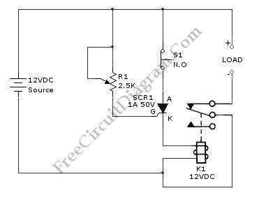
An overvoltage protector circuit is shown in the schematic diagram below. This circuit will work to disconnect the protected device from the power supply when an overvoltage occurs at the supply. This circuit uses a silicon-controlled rectifier (SCR) and normally-closed 12-V relay, K1. The silicon-controlled rectifier is connected in parallel to 12-V line to monitor for the overvoltage condition. This applied signal is sensed by the SCR’s gate. Here is the schematic diagram of the circuit:
The K1′s contacts remain closed and SCR1 remains off as long as the applied voltage stays below a preset value. When overvoltage occurs, the SCR1 will be triggered causing K1′s contacts open and halt current flow to the load. R1 is used to set the trigger point of SCR1.(source: freecircuitdiagram)
(View)
View full Circuit Diagram | Comments | Reading(1700)
Logic Power Control for 78xx Regulator
Published:2012/9/4 1:28:00 Author:Ecco | Keyword: Logic Power Control, Regulator
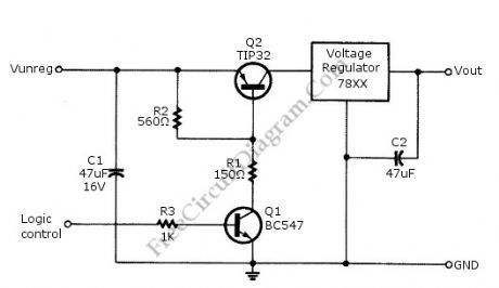

Logic power control of analog regulator can be useful in application where a digital circuit/controller need to control power source, such as in EEPROM programmer or other power controls. This is a circuit provide ON-OFF control for 78xx regulator using digital (TTL or CMOS) signal level. This circuit uses transistors in series with the 78XX regulator, which it’s base is controlled by logic level input. Here is the schematic diagram of the circuit: (source: freecircuitdiagram)
(View)
View full Circuit Diagram | Comments | Reading(1690)
Variable Frequency Switch Mode Regulator
Published:2012/9/4 1:26:00 Author:Ecco | Keyword: Variable Frequency , Switch Mode, Regulator

This voltage regulator circuit operates in switch mode. Using the configuration shown in the schematic diagram, this circuit has variable switching frequency, depends on the input voltage and load condition. The core controller of this switching regulator is a TL497 switching regulator controller IC. Here is the schematic diagram of the circuit: (source: freecircuitdiagram)
When the load is low (draw only small current), this circuit will lower the frequency to give lower active factor, keeping the output voltage at constant level. When the load draw higher current then this regulator circuit will produce higher switching frequency to compensate the faster drop output capacitor (100uF). You can see that the voltage of this output is sense through voltage divider resistors (3.3k and 1.2k), we can tune this resistor to give other than 5V output voltage. A 75% efficiency is possible to achieve with this switching regulator circuit.
(View)
View full Circuit Diagram | Comments | Reading(1870)
Black Light (UV Tube Lamp) Inverter
Published:2012/9/4 1:21:00 Author:Ecco | Keyword: Black Light, UV Tube Lamp, Inverter
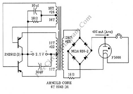
The voltage boosting in this circuit enable its operation to be powered by 2.5 V rechargeable battery (two cells 1.2V rechargeable batteries), supplying 400 mA current at 26 V which is needed by the gas arc tube for portable ultraviolet lamp. This inverter circuit has a good efficiency as well, about 80%. Ultraviolet (UV) light is also known as black light since the light is invisible, but can energize some materials to glow when the materials is exposed to this black light. Money or other security tag is usually checked used this kind of light. Here is the schematic diagram of the circuit: (source: freecircuitdiagram)
(View)
View full Circuit Diagram | Comments | Reading(2321)
Power Saver for Relays
Published:2012/9/4 1:18:00 Author:Ecco | Keyword: Power Saver , Relays

Relays are normally operated at current level where it can initiate the mechanical metal contactors movement. After contacts has been established, the current level needed to keep the conductor plates stay attached is actually smaller than the current to initiate it. This power saver circuit seems to have opposite mechanism of surge protector. This circuit provide surge current to initiate mechanical movement, but after that, this circuit throttle the current to save the power, provide lower current level just to keep the contacts stay attached. Here is the schematic diagram of the circuit:
The mechanism of this circuit is similar but done in opposite way with current surge protector. If we use a varistor with negative coefficient, here we use a kind of varistor but with positive coefficient, where the resistance increases as the temperature increase. This kind of varistor is actually an incandescent bulbs, two bulbs in parallel. At cold temperature, this bulbs has very low resistance, this make sure the relay will has sufficient power supply to initiate the mechanical movement of its contactors. After the relay works, the rise of bulbs temperature will make the current decreased to a lower level, saving the power while maintaining the contactors stay attached. That’s all the mechanism of this power saver circuit.
(source: freecircuitdiagram)
(View)
View full Circuit Diagram | Comments | Reading(1249)
Selectable Voltages 6V, 9V, and 12V Linear Voltage Regulator
Published:2012/9/4 1:16:00 Author:Ecco | Keyword: Selectable Voltages, 6V, 9V, 12V , Linear Voltage Regulator
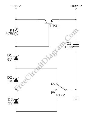
We can build a multiple voltage power supply 6, 9, and 12V (AC-DC Adapter) with the circuit shown in the following schematic diagram. Not only provide multiple voltage output with single voltage supply, this circuit add the benefit of regulating the voltage for better stability. The TIP31 transistor should be installed with proper heat-sink to prevent overheating. A transformer with rectifier diodes and filtering capacitor can be used to supply this circuit. You can use 1 A 15V transformer with 2200uF filtering capacitor for the AC to DC adapter. (source: freecircuitdiagram)
(View)
View full Circuit Diagram | Comments | Reading(2013)
Automotive/Car Power Adapter For 3V, 6V, or 9V DC Operated Devices
Published:2012/9/4 1:14:00 Author:Ecco | Keyword: Automotive, Car Power Adapter , 3V, 6V, 9V, DC Operated Devices
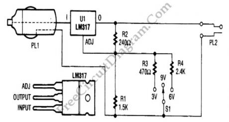
In automotive environment, it’s common that only single voltage power outlet is available. Using the very popular LM317 voltage regulator IC, we can build a general purpose DC adapter to adapt car’s power outlet voltage (12-14 Volts) to supply small DC devices requiring lower voltage level. On the following schematic diagram for the car power adapter, we can see that the output voltage depends on the value of R1, which is manipulated by connecting R3 or R4 via switch to program the output. When connected through the switch, R1 will be in parallel with the selected resistor so the total resistance changes to affect the output voltage.
(View)
View full Circuit Diagram | Comments | Reading(3190)
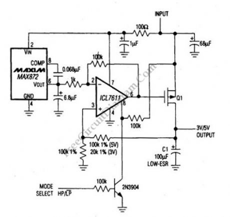
Three Cells Produce Regulated 3V – 3.3V
Published:2012/9/4 1:11:00 Author:Ecco | Keyword: Three Cells , Regulated 3V – 3.3V
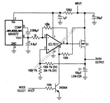
Three NiCad and NiMH batteries can be used to produce 3V/3.3V supply voltage. This can be done by this linear regulator circuit. This circuit uses an ICL7611 micropower op amp and MAX872 voltage reference. This regulator can be used to replace the charge pump or a switching regulator. The dropout characteristics of this circuit depends on the characteristics of Q1. The Q1 must have a gate-threshold voltage below the lowest battery voltage when this circuit is used with low voltage like a three-cell battery. Here is the schematic diagram of the circuit: (source: freecircuitdiagram)
This circuit requires input voltage from 3V to 15V. This circuit has two mode, high power mode and low power mode that can be selected by logic at the MODE SELECT input. With Vin 6.5V, the quiescent current is 70µA when operated in high power mode and decrease to 40µA when it is used in low power mode. This circuit has maximum load power of 5mA in low power mode and 1A in high power mode.
(View)
View full Circuit Diagram | Comments | Reading(1066)
Ni-Cad Battery Zapper, A Rechargeable Battery Reconditioner
Published:2012/9/4 1:09:00 Author:Ecco | Keyword: Ni-Cad Battery Zapper, Rechargeable , Battery Reconditioner

Ni-Cad (NiCd, NiCad) battery, sometimes doesn’t work as expected, gives no power and cannot be recharged. In this situation, the battery need to be reconditioned. It’ is possible that the battery is internally shorted, and we can get the battery into life again by recondition the Ni-Cad battery using a zapper circuit. This circuit restore the Ni-Cad battery from shorting by forcing a high current flow to burn the internal dirt. The current stored in the high capacitance capacitor is heavy discharged by the SCR when zapping, and the SCR is used to disconnect the battery connection when charging the capacitor. A 120 ohm 10W resistor is used to limit the current when charging the capacitor, and you have to make sure the LED’s intensity has reach the steady state before switching to zap position. After zapping the battery and switch to charge position, the charging process will take some period and indicated by the LED which will gradually increase the brightness until get stable intensity when fully charged. The power supply for this circuit can be taken from small transformer (350 mA to 1 A) with half or full wave rectifier. Here is the schematic diagram of the battery zapper circuit: (source: freecircuitdiagram)
(View)
View full Circuit Diagram | Comments | Reading(1255)
Main Power-Battery Backup Switcher
Published:2012/9/4 1:08:00 Author:Ecco | Keyword: Main Power-Battery , Backup Switcher
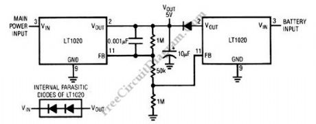
The schematic diagram shown below is a battery backup regulator circuit, useful for memory or other low power (battery operated) but critical circuit (must continue operation on powerline failure). The one LT020 will not conduct in under line-powered condition, made possible by means of of feedback string’s arrangement. In case of main power failure, the battery-driven LT1020 will turn on and maintain the load, when the line LT1020 go off because the line goes down. Here is the schematic diagram of the circuit: (source: freecircuitdiagram)
(View)
View full Circuit Diagram | Comments | Reading(974)
High-Voltage Generator with HEX FET
Published:2012/9/4 1:07:00 Author:Ecco | Keyword: High-Voltage Generator , HEX FET
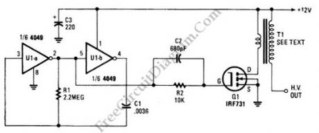
The schematic diagram below show a circuit of high voltage generator. This circuit uses a 4049 hex inverter as an oscillator, and you can use ignition transformer from automotive engine. A fly-back transformer is possibly usable too. The 4049 will drive the IRF731 HEX FET. The Q1 must be heatsinked. Here is the schematic diagram of the circuit: (source: freecircuitdiagram)
(View)
View full Circuit Diagram | Comments | Reading(3217)
TLC497CN Negative Supply Generator
Published:2012/9/4 1:05:00 Author:Ecco | Keyword: Negative Supply Generator
Three NiCad and NiMH batteries can be used to produce 3V/3.3V supply voltage. This can be done by this linear regulator circuit. This circuit uses an ICL7611 micropower op amp and MAX872 voltage reference. This regulator can be used to replace the charge pump or a switching regulator. The dropout characteristics of this circuit depends on the characteristics of Q1. The Q1 must have a gate-threshold voltage below the lowest battery voltage when this circuit is used with low voltage like a three-cell battery. Here is the schematic diagram of the circuit:( source: freecircuitdiagram)
This circuit requires input voltage from 3V to 15V. This circuit has two mode, high power mode and low power mode that can be selected by logic at the MODE SELECT input. With Vin 6.5V, the quiescent current is 70µA when operated in high power mode and decrease to 40µA when it is used in low power mode. This circuit has maximum load power of 5mA in low power mode and 1A in high power mode. (View)
View full Circuit Diagram | Comments | Reading(1144)
Passive Aircraft Receiver
Published:2012/8/29 2:08:00 Author:jailer | Keyword: Aircraft Receiver
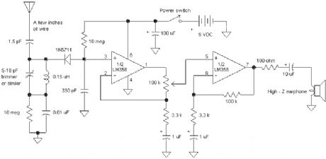
The Passive Aircraft Receiver is basically an amplified crystal radio designed to receive nearby AM aircraft transmissions. The passive design uses no oscillators or other RF circuitry capable of interfering with aircraft communications so it should be fine inside the cabin of the aircraft. Nevertheless, check the regulations before using this receiver on a commercial airliner. New security regulations probably prohibit this device on commercial flights. Do not expect to hear two-way aircraft transmissions with this receiver! It is a short-range receiver only.
The detector diode is a 1N5711, HP2835 or similar Schottky detector diode. The 10 megohm resistors provide a small diode bias current for better detector efficiency. The tuning capacitor may be any small variable with a range from about 5 pF to about 15 or 20 pF. The 0.15 uH inductor may be a molded choke or a few turns wound with a small diameter. Experiment with the coil to get the desired tuning range. The aircraft frequencies are directly above the FM band so a proper inductor will tune FM stations with the capacitor set near maximum capacity. (The FM stations will sound distorted since they are being slope detected.) Other capacitor and inductor combinations may be selected to tune other bands if desired. (Try the CB band at 27 MHz.) The LM358 dual op-amp draws under 1 ma so the battery life is quite long. A speaker amplifier may be added to drive a speaker or low-z earphone. The antenna can be a couple of inches if the receiver is near the transmitter or a couple of feet for maximum range. The selectivity is reduce as the antenna length is increased so best performance is achieved with the shortest acceptable antenna. Try increasing the 1.8 pF capacitor value when using very short antennas and decreasing it for long antennas. The receiver could be built into a small plastic box with a short antenna inside. (View)
View full Circuit Diagram | Comments | Reading(2210)
Single supply +5 V operating circuit of logarithmic and logarithmic ratio amplifier LOG101/104
Published:2012/8/22 20:50:00 Author:Ecco | Keyword: Single supply , +5 V , operating circuit , logarithmic , logarithmic ratio , amplifier
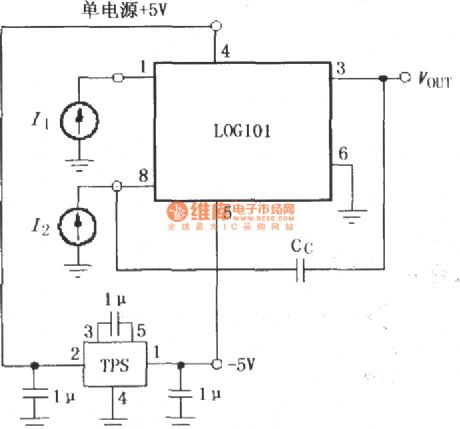
Many applications only have a single power supply, while LOG101/104 needs dual power. The circuit shown in figure uses a negative pump power TPS6040DBV which can switch a single +5 V power supply to a -5V supply for LOG101/104.
(View)
View full Circuit Diagram | Comments | Reading(946)
Three-terminal integrated voltage regulator constant current source circuit
Published:2012/8/12 21:00:00 Author:Ecco | Keyword: Three-terminal , integrated , voltage regulator , constant current source
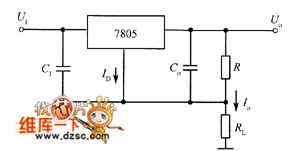
Figure 1 shows the constant current source circuit composed of 7805. Resistor R is connected at the output and public ends to form a fixed constant current, then thecurrent flows through the load RL and then back to power supply. Regulator works in the suspended state. The circuit uses regulator to change its own differential pressure to maintain constant current flowing through the load when the load changes. Output current Io = 5V / R 10 ID,in the formula, ID = 1.5mA ( using 7805 , ID = 1.5mA ). Therefore, changing the size of the R can adjust output current.
(View)
View full Circuit Diagram | Comments | Reading(2114)
3.6W mobile phone battery charger circuit diagram
Published:2012/8/12 20:47:00 Author:Ecco | Keyword: 3.6W , mobile phone , battery charger
The3.6W charger circuit special for mobile phone is shown as the figure, andthe power supplyhas constant current / constant voltage output characteristics, and the no-load power consumption is less than 100mW. It can provide constant current charging for nickel-metal hydride (NiMH) batteries or nickel cadmium (NiCd) batteries, lithium ion ( Li = ion) batteries inmobile phone. Its main technical index: AC input voltage u = 85 ~~ 265V, output voltage Uo = 5.2V , the maximum output current Iom = 0.697A, output power Po, = 3.6W.
(View)
View full Circuit Diagram | Comments | Reading(4980)
LED power supply voltage-doubler circuit
Published:2012/7/18 3:23:00 Author:Ecco | Keyword: LED , power supply , voltage-doubler circuit
The power supply voltage-doubler conversion circuit is shown as the figure. Some amplifiers require small current and high voltage in electronic circuit designs, so the power supply voltage-doubler conversion circuit composed of flashing light-emitting diodes and a small number of components can be used. In Figure (a), the capacitors C1, C2 can be used to storage charge, and the circuit uses the oscillation of flashing light-emitting diode to drive relay switch for conversion, then C1 and supply voltage are superimposed to obtain twice of power supply voltage on C2. The output current of circuit is about 10mA. Relays uses 6V , 30mA types. The figure (b) is a voltage doubler schematic diagram.
(View)
View full Circuit Diagram | Comments | Reading(1676)
The power output circuit diagram with automatic drive mode
Published:2012/7/16 3:12:00 Author:Ecco | Keyword: power output , automatic drive mode
The output voltage of the system in the design is 3.3 V , and it uses automatic drive mode. It usesthe secondary of transformerto drive MOSFET. When the circuit works, the transformer's secondary is in positive hafle circle, V8 is breakover, V9 is turned off, and V8 plays the role of rectifying action. When transformer's secondary is in negative half cycle , V9is breakover, V8isturn off, V9 has the freewheeling function. As shown in Fig, when it works under the condition of 300 kHz , the loss of the synchronous rectifier is conduction loss, and the switching loss is small.
(View)
View full Circuit Diagram | Comments | Reading(1082)
Regulated power supply application circuit diagram
Published:2012/7/3 21:42:00 Author:Ecco | Keyword: Regulated power supply , application
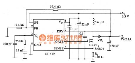
Figure a, b show the application circuits of LT1619 and LT1767. Figure (a) is the application circuit of the LT1619. It is the current controller, and it can be used as step-up inductive single-ended converter and flyback converter when the external components is rare. LTl619's external components is rara, which has small size with high efficiency. LTl619 can converter the input voltage of 3.3V to 5V/2.2A output. Under heavy load, the conversion efficiency is higher than the other converters, and the voltage on the current sense resistor drops to only 5OmV with samll resistor power loss, resulting in improved conversion efficiency. When the load is light, it works with burst way to maintain high conversion efficiency. The typical operating frequency is 300kHz. When it is in synchronization with external clock, the operating frequency can get 5OOkHZ. No-load current is 14OμA, while standby current is only 15μA.
(View)
View full Circuit Diagram | Comments | Reading(1525)
BQ2000 charge controller
Published:2011/12/1 21:23:00 Author:May | Keyword: charge controller
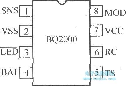
BQ2000 charge controller is pioneer product currently inpower source technology field. It intergrates each element circuit charge controller needed in one IC. The arithmetic unit in the chip can make the whole circuit control be more precise, operation bemore safe, function be more complete. Its pin array is shown in the following diagram.
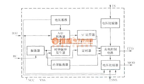
The internal functional block diagram is shown in the following diagram:
(View)
View full Circuit Diagram | Comments | Reading(2015)
| Pages:48/291 At 204142434445464748495051525354555657585960Under 20 |
Circuit Categories
power supply circuit
Amplifier Circuit
Basic Circuit
LED and Light Circuit
Sensor Circuit
Signal Processing
Electrical Equipment Circuit
Control Circuit
Remote Control Circuit
A/D-D/A Converter Circuit
Audio Circuit
Measuring and Test Circuit
Communication Circuit
Computer-Related Circuit
555 Circuit
Automotive Circuit
Repairing Circuit