
Analog Circuit
Index 19
ANTENNA_TUNER
Published:2009/6/18 23:18:00 Author:May
This is a circuit diagram of the Collins Model 1805-1 antenna tuner. Three unbalanced configurations are available, two of which form an L-network and the other is a π-network. The tuning range is impressive. (View)
View full Circuit Diagram | Comments | Reading(124)
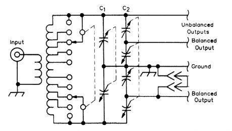
MATCHBOX_ANTENNA_TUNER
Published:2009/6/18 23:17:00 Author:May

C1 is a split stator capacitor and C2 is a dual differentiaJ capacitor. The top unbalanced output connection is used for high-impedance unbalanced loads, and the other is used for low-impedance unbalanced loads. In the latter case, the unused balanced load connection is grounded. (View)
View full Circuit Diagram | Comments | Reading(1119)
FM_AUTO_RADIO_DIVERSITY_ANTENNA
Published:2009/6/18 23:08:00 Author:May


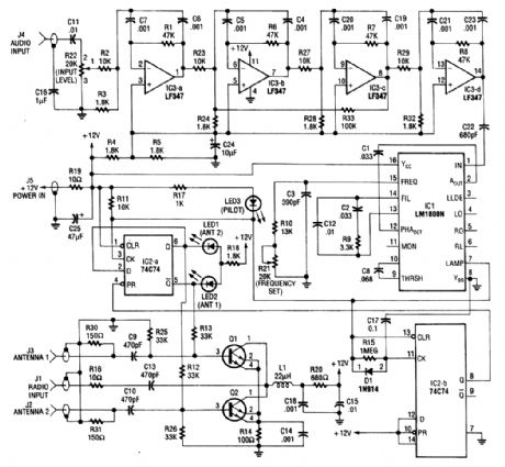
A second antenna, installed on your vehicle as far away from the original equipment antenna as practical, provides the second FM signal. The figure is a simplified block diagram of the diversity system.The cables from both antennas are connected to the electronic antenna switch. The 19-kHz pi-lot signal from the receiver's audio output is passed through a high-gain bandpass active filter, which attenuates audio programming that is much stronger than the pilot signal. After amplification, the pi-lot subcarrier becomes the reference frequency for a phase-locked loop (PLL) circuit. The output of the PLL locks to the 19-kHz pilot signal and functions as a subcarrier detector. When the reference frequency becomes noisy, the PLL will lose lock and trigger the flip-flop, whose output switches the state of the electronic antenna switch,This action switches the alternate antenna into the system while disabling the original antenna.
If that second antenna is positioned for better reception,the received signal will clear,and the PLL will again lock to the subacrrier and hold the switch in that state until the pilot signal drops out again,If the second antenna does not restore the pilot signal reception after a0.1-second delay,the primary antenna is switched back on.When the radio is receiving AM, the absence of the 19- kHz subcarrier will also reactivate the primary antenna that is tuned to the receiver tor the best AM reception. (View)
View full Circuit Diagram | Comments | Reading(1714)
MINIATURE_BROADBAND_ANTENNA_3_TO_30_MHz
Published:2009/6/18 23:06:00 Author:May
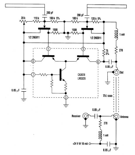
A short dipole antenna and impedance converter combined together can be rotated to null out an interfering signal. The converter supplies a tremendous current gain so that the voltage appear-ing at the dipole's output eventually drives a 75-Ω load. (View)
View full Circuit Diagram | Comments | Reading(1248)
REMOTE_TUNED_ACTIVE_HF_ANTENNA
Published:2009/6/18 23:04:00 Author:May
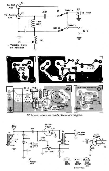
An MV1662/S varactor diode tunes this active antenna/preamplifier.R1 varies gate bias on the BS170 FET. T1 is a 3:1 toroidal winding suitable for the frequencies of interest. (View)
View full Circuit Diagram | Comments | Reading(2816)
ELECTRONIC_GONG
Published:2009/6/18 22:59:00 Author:May
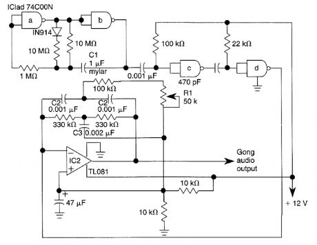
The electronic gong is comprised of an oscillator (built around half of a 74COON quad 2-input NAND gate), an active twin-T filter (built around a TL081), and will drive an audio amplifier IC such as an LM386N. Pulses from astable multivibrator IC1 cause the twin-tee active filter U2 to ring, producing a damped sinusoidal output. C1 varies rate and C2-C3 vary gong frequency. Adjust RI for best tone sound. (View)
View full Circuit Diagram | Comments | Reading(3411)
AUTOMATIC_FADER
Published:2009/6/18 22:25:00 Author:May
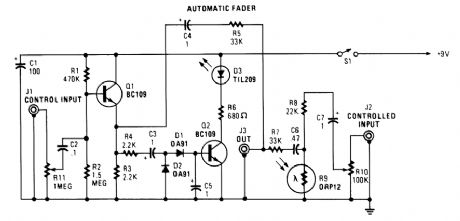
In this circuit, audio fed to the control channel is amplified and rectified by D1 and D2. This dc level activates LED D3 via Q2. The light from D3 causes R9, a light-dependent resistor to decrease resistance. As R11 (audio gain) is set higher, more audio is present at the output of Q1. Audio fed into J2 is shunted to ground via R9 and less of this audio appears at J3. Therefore, audio at J1 controls the audio level fed to J3 from J2 and produces a fade effect. (View)
View full Circuit Diagram | Comments | Reading(817)
SONIC_KALEIDOSCOPE
Published:2009/6/18 22:16:00 Author:May
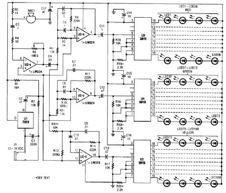
The microphone input, MIC1, is fed through C3 and R4 to inverting amplifier U2-a; the gain of U2-a is controlled by potentiometer R5. The output of U2-a is fed through C4 to the remaining op-arnps (U2-b, U2-c, U2-d), which are all configured as band-pass filters. Each filter is tuned to pass a different range of frequencies by its resistor/capacitor combination. With the values shown, U2-b, U2-c, and U2-d have center frequencies of roughly 100, 1000 and 1500 Hz, respectively.Resistors R6, R9, R12 control the bandwidth and gain of their respective filter circuits, and can range in value from 10 to 15 kΩ. The output of U2-b is capacitively coupled via C11 to the input of U3, with R15 serving as the load resistor for U2-b. That resistor also keeps U3's outputs from float-ing in the absence of a signal. Connected as shown, U3 uses its own internal voltage reference to make a full-scale display of 1.2 V.Each ofthe nlne outputs of U3(output 1 IS not used) sinks four, series-connected (red) LEDs. Op amps U2-c and U2-d qro similarly connected to U4 and U5,respectively, driving green and yellow LED strings,Resistors R18,R19,and R20 control the brightness of their corresponding LED arrays,and they must be adjusted accordingly;different colors of LEDs usually vary in brightness.A lowervalue of resistance will make the LEDs glow brighter.Power for the circuit is supplied by a 500 mA,12-15-Vdc wall-pack transformer,via J1 The out-put ofthe transformer is filtered by 01 arid is regulated by U1;regulation is necessary to keep power-line ripple from affecting the display. The Supply pins of U2 through TTKLJt are bypassed by capacitors014 through C17 to further ensure stability. An on/off switch was deemed unnecessary because thepower Supply should be unplugged when the unit is not in use. (View)
View full Circuit Diagram | Comments | Reading(1014)
VOCAL_STRIPPER
Published:2009/6/18 22:06:00 Author:May
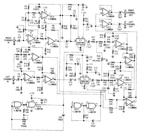


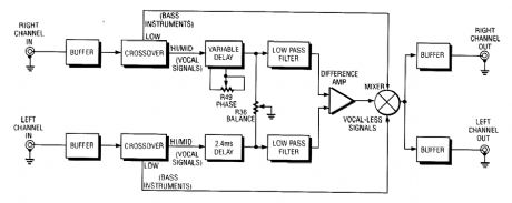
Right- and left-channel signals pass through 1 C4-a and -b buffer amps into active crossover IC5; low frequencies are sent to the ICG-c mixer, and middle and high frequencies are sent to the analog delay lines of 1C1 and 102. That output passes through 1C6-a and -d to filter high-frequency sample steps. IC6-b signals are remixed with low frequencies by ICG-c and are sent to final out via IC4-c and -d buffers.One channel (R) is a variable-delay circuit, using an analog bucket-brigade device and a variable clock frequency. This is compared in amplitude and phase to the L channel (fixed delay). The local can therefore be nulled out via R36. (View)
View full Circuit Diagram | Comments | Reading(1602)
ISD_1000A_RECORD_PLAYBACK_CIRCUIT
Published:2009/6/18 22:00:00 Author:May


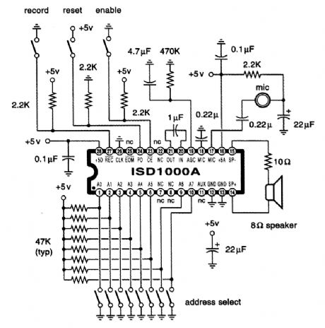
This circuit uses the Information Storage Devices ISD1000A chip(Radio Shack P/N 276-1325). (View)
View full Circuit Diagram | Comments | Reading(2885)
SIMPLE_ANALOG_MULTIPLIER
Published:2009/6/18 21:50:00 Author:May
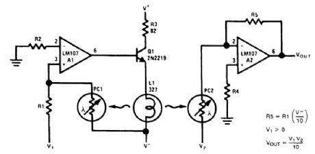
Circuit operation can be understood by considering A2 as a controlled-gain amplifier, amplifying V2, whose gain depends on the ratio of the resistance of PC2 to R5 and by considering A1 as a control amplifier, which establishes the resistance of PC2 as a function of V1. In this way, VOUT, is a function of both V1, and V2.A1, the control amplifier, provides drive for the lamp, L1. When an input voltage, V1, is present, L1 is driven by A1 until the current to the summing junction from the negative supply through POI is equal to the current to the summing junction from V1 through R1. Because the negative supply voltage is fixed, this fordes the resistance of PCl to a value that is proportional to R1 and to the ratio of V1, to V-. L1 also illuminates PC2 and, if the photoconductors are matched, causes PC2 to have a resistance equal to PC1.A2, the controlled gain amplifier, acts as an inverting amplifier whose gain is equal to the ratio of the resistance of PC2 to R5. If R5 is chosen equal to the product of R1, and V-, then VOUT becomes simply the product of V1, and V2. R5 can be scaled in powers of 10 to provide any required output scale factor. (View)
View full Circuit Diagram | Comments | Reading(1785)
SIMPLE_ANALOG_AVERAGING_CIRCUIT
Published:2009/6/18 21:34:00 Author:May

At times,an analog circuit that averages rather than sums call be quite handy. You won’t usually find this type of circuit in op-amp books,possibly because the op amp is used only as a buffer Forbest accuracy,an FET should be used with the offset adjusted out.In addition,the“averagtng”resistors(R1 through R4)should be of Close tolerance.Looldng at the test circuit,op amps 1 through 4 are used to alleviate interaction between adjustment potentiometers P1 through P4 and so that R1 through R4 see the same low impedance.The table shows some arbitrarily set voltages and the resulting output voltage across RL. (View)
View full Circuit Diagram | Comments | Reading(864)
SUBCARRIER_ADAPTER_FOR_FM_TUNERS
Published:2009/6/18 21:32:00 Author:May
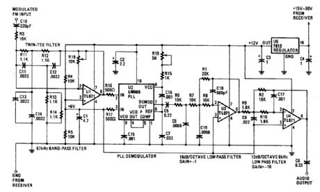
Op amp U1 and its associated components comprise the 67-kHz bandpass filter. A twin-T net-work, comprised offour 1100-Ω resistors and four 0.0022-pF capacitors, is connected in the feed-back network of the op amp. That gives some gain at 67 kHz and heavy attenuation for frequencies above and below that frequency.An additional passive filter at the input to the twin-T network (containing a 220-pF capacitor and a 10,000-Ω resistor) provides some additional roll-off for frequencies below 67 kHz.In practice, the bandpass-filter action covers a frequency range of about 10 kHz above and below the 67-kHz center frequency. Resistor R18 sets the gain of the bandpass-filter stage.Integrated-circuit U2 is a National LM565 phase-locked loop that modulates the 67-kHz fre-quency-modulated (FM) signal from U1. The LM565 PLL consists of a voltage-controlled oscillator (VCO) set to 67 kHz, and a comparator that compares the incoming frequency-modulated 67-kHz signal at pin 2 with the VCO signal that is fed into pin 5.The output of the comparator represents the phase difference between the incoming signal and the VCO signal. Therefore, the output is the audio modulated by the subcarrier. A treble deemphasis of 150 ps is provided by a 0.033-μF capacitor (at pin 7).The free-running VCO frequency is determined by the 0.001-μF capacitor at pin 9 and by the re-sistance between the positive rail and pin 8 (100 Ω in series with R19). Variable-resistor R19 adjusts the oscillator frequency (also known as the centerfrequency) so that the incoming signal is within the lock range of the PLL. (View)
View full Circuit Diagram | Comments | Reading(1107)
DIFFERENCE_OF_SQUARES
Published:2009/6/18 21:20:00 Author:May
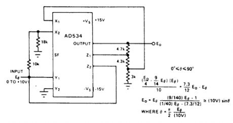
The AD534 is remarkably easy to use in the implementation of the approximation formulas described in Chapter 2-1 of the NonLinectr Circuits Hctndbook. Many of these involve implicit loops to generate the function and previously required several additional op amps for the addition and subtraction of the various terms. This circuit is an example of what can be done with extemal resistors only. For φ between 00 and 900, the approximation maintains a theoretical accuracy to within 0.5% of fullscale; 0.75% is practical with AD534L and 0.1% resistances were used. (View)
View full Circuit Diagram | Comments | Reading(800)
ANALOG_VARIABLE_MULTIPLIER_DIVIDER
Published:2009/6/18 21:09:00 Author:May
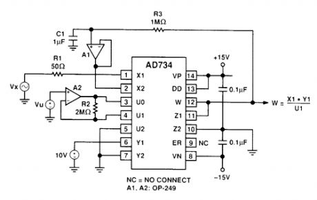
An output voltage (W=X1×Y1/U1) is produced by Lhis multiplier circuit The AD734 is a fourquadrant multiplier. (View)
View full Circuit Diagram | Comments | Reading(997)
SQUARE_ROOTER
Published:2009/6/18 21:03:00 Author:May
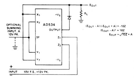
This illustration shows the connection of the AD534 for square-rooting, with differential inputs.The diode prevents a latching condition-common to this conftguration-which would occur if the input momentarily changed polarity. As shown, the output is always positive; it can be changed to a negative output by reversing the diode polarity and interchanging the X inputs. Because the signal input is differential, all combinations of input and output polarities can be realized. If the output circuit does not provide a resistive load to ground, one should be connected to maintain diode conduc-tion. For critical applications, the Z offset can be adjusted for greater accuracy below1 V. (View)
View full Circuit Diagram | Comments | Reading(878)
BRIDGE_LINEARIZING_FUNCTION
Published:2009/6/18 20:57:00 Author:May
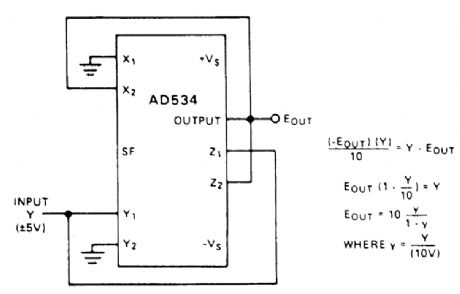
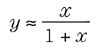
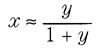
If one arm of a Wheatstone Bridge varies from its nominal value by a factor,(1 + 2x), the voltage or current output of the bridge will be(with appropriate polarities):Linear response requires very small x and,usually,prearrtplification.The circuit shown here enables Iarge-deviation bridges to be used without losing linearity.The circuit computes the inverse of the bridge function, i.e.,Depending on which arm of the bridge varies, it might be necessary to reverse the polarity of the z connections. (View)
View full Circuit Diagram | Comments | Reading(771)
ULTRA_LOW_DISTORTION±50_mA_DRIVER
Published:2009/6/18 4:57:00 Author:May
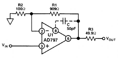
For a 600-Ω load,THD is typically-115 dB at 20 kHz,3-V RMS output,、with±15-V supplies The-3-dB BW is 6 MHz. (View)
View full Circuit Diagram | Comments | Reading(840)
COAX_CABLE_DRIVER
Published:2009/6/18 4:56:00 Author:May
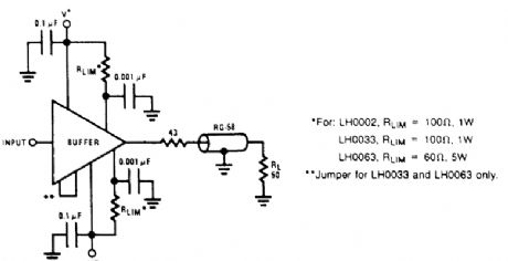
Becbuse of their high-current drive capability, the LH0002, LH0033, and LH0063 buffer ampli-fiers are suitable for driving terminated or unterminated coaxial cables, and high-current or reactive loads. Current-limiting resistors should be used to protect the device from excessive peak load cur-rents or accidental short circuit. No current limiting is built into the devices other than that imposed by the limited beta of the output transistors. This figure shows a coaxial-cable drive circuit. The 43-Ω resistor is included, the output voltage to the load is about half what it would be without the near-end termination. (View)
View full Circuit Diagram | Comments | Reading(1386)
VIDEO_CABLE_DRIVER
Published:2009/6/18 4:55:00 Author:May
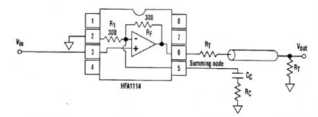
The driver's frequency response is tunable for a specific cable length via components connected to the summing node. By shunting R1,RC, acts to increase the amplifier's gain, and CC controls the cut-in frequency of the compensation.These three components peak the amplifier's frequency response to counteract the cable's roll-off characteristic. By squeezing more bandwidth out of a given cable, higher-performance cables aren't needed. (View)
View full Circuit Diagram | Comments | Reading(0)
| Pages:19/24 1234567891011121314151617181920Under 20 |
Circuit Categories
power supply circuit
Amplifier Circuit
Basic Circuit
LED and Light Circuit
Sensor Circuit
Signal Processing
Electrical Equipment Circuit
Control Circuit
Remote Control Circuit
A/D-D/A Converter Circuit
Audio Circuit
Measuring and Test Circuit
Communication Circuit
Computer-Related Circuit
555 Circuit
Automotive Circuit
Repairing Circuit