
Electrical Equipment Circuit
Index 59
PREFERRED_AMPLIFICATION_300_PREAMPLIFIER
Published:2009/7/23 23:43:00 Author:Jessie
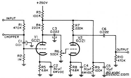
Used with instrument servo motor controller to increase available gain. Chopper is used with d.c inputs only.-NBS, Handbook Preferred Circuits Navy Aeronautical Electronic Equipment, Vol. I, Electron Tube Circuits, 1963, PC 73, p 73-2. (View)
View full Circuit Diagram | Comments | Reading(733)
Comparator_logic_level_translator_TTL_to_CMOS
Published:2009/7/24 4:52:00 Author:Jessie
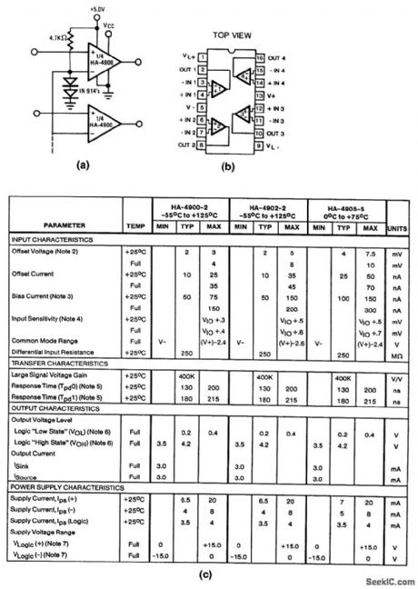
Fig. 15-32 This circuit shows two sections of an HA-4900 used as a TTL to CMOS interface. Additional sections can be added. Negative logic devices may also be interfaced with appropriate supply connections, If separate supplies are used for V- and YLOGIC-, this circuit will tolerate several volts of ground-line differential noise. Figures 15-32B and 15-32C show the pin connections, and electrical characteristics, respectively. Harris Semiconductor Linear & Telecom ICs, 1991 p, 4-24 4-25, 4-29. (View)
View full Circuit Diagram | Comments | Reading(846)
PEAK_VOLTMETER_FOR_NARROW_PULSES
Published:2009/7/24 0:01:00 Author:Jessie
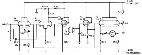
Addition of dual-triode amplifier V2 to conventional peak voltmeter reduces charging time constant while increasing available time for measuring peak value. Linearity is good up to 40 v.-M. Uno, Amplifier Improves Peak Voltmeter Response, Electronics, 37:14, p 73. (View)
View full Circuit Diagram | Comments | Reading(784)
ON_OFF_RELAY_SERVO
Published:2009/7/24 Author:Jessie
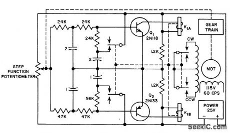
Step-function potentiometer provides on-off characteristic of null detector. Easily adjusted damping is applied through differential relay contacts to eliminate oscillations. Fast response to small angular displacements assures dose following. Tapping positive voltage off stop-function potentiometer causes current low through Q1, operation of relay K1A, and upward movement of arms. Negative voltage moves arms downward, reversing motor travel.-S. Shenfeld, Transistors Reduce Relay Servo Size, Electronics, 31:33, p 74-77. (View)
View full Circuit Diagram | Comments | Reading(1008)
TWO_SPEED_SERVO
Published:2009/7/23 23:56:00 Author:Jessie
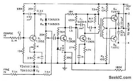
Directly drives size 11 motor, eliminating need for output transformer. Zener diodes provide switching between fine and coarse signals for two speeds. Maximum coarse and One signal input is 26 V rms at 400 cps. Voltage gain of coarse amplifier Q1 is 25, and gain of feedback amplifier Q2-Q3-Q4-Q5 is 460.-B. E. Orr, Direct Drive Amplifier for Two-Speed Servos, Electronics, 31:11, p 146-147. (View)
View full Circuit Diagram | Comments | Reading(839)
PREFERRED_RESOLVER_DRIVER
Published:2009/7/23 23:59:00 Author:Jessie
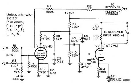
A-c operational amplifier is used as isolation amplifier, employing feedback that includes compensating winding of a-c resolver being driven. Useful as computing element for coordinate conversion, coordinate rotation, and resolution of vectors when accuracy of 0.5% is sufficient. Component values given are for 500 cps, with Mark 4 Mod 0 resolver.-NBS, Handbook Preferred Circuits Navy Aeronautical Electronic Equipment, Vol. I, Electron Tube Circuits, 1963, PC 79, p 79-2. (View)
View full Circuit Diagram | Comments | Reading(799)
Transition_slew_rate_tests
Published:2009/7/23 23:56:00 Author:Jessie
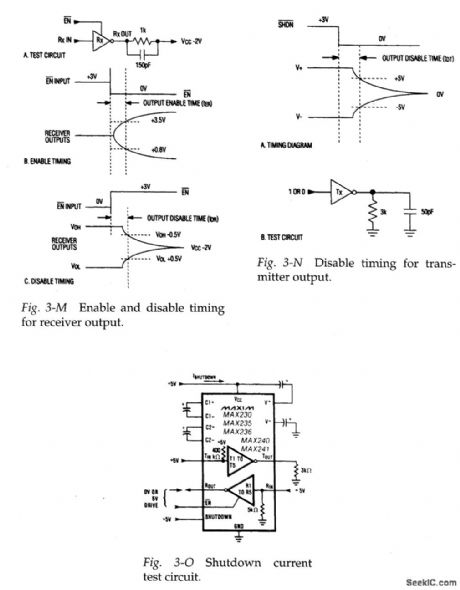
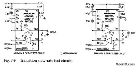
Figure 3-P shows a transition slew-rate test circuit for the MAX200/11/13. (Slew rate is covered in Chapter 6.) For reference, the slew rate is 5.5V/μs (typical) and 30V/μs (maximum) for the ICs involved. (View)
View full Circuit Diagram | Comments | Reading(799)
Isolated_RS_485_RS_422_data_interface
Published:2009/7/24 0:02:00 Author:Jessie

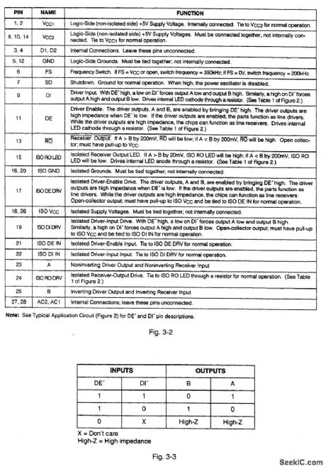
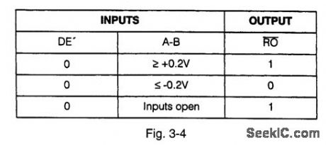
Figure 3-1 shows the typical application circuit for the MAX1480A/B. These ICs are complete, electrically isolated RS-485/RS-422 data-communications interfaces. Transceivers, opto-couplers, and a transformer provide a complete interface in one 28-pin package. Figure 3-2 shows the pin descriptions. Figures 3-3 and 3-4 show the function tables. The MAX1408B has reduced-slew-rate drivers that minimize EMI (electromagnetic interference) and reduce reflections caused by improperly terminated cables, allowing error-free data transitions at data rates up to 250 kbps. The MAX1480 driver slew rate is not limited, allowing transmission rates up to 2.5 Mbps. The ICs draw 28 mA of quiescent current. The MAX1408B provides a low-power shutdown mode that consumes only 0.2μA. The drivers are short-circuit current-limited and are protected against excessive power dissipation by thermal shutdown circuits that place the driver outputs into a high-impedance state. The receiver input has a fail-safe feature that guarantees a logic-high output if the input is open circuit. The ICs typically can withstand 1600 Vrms for one minute or 2000 Vrms for one second. MAXIM NEW RELEASES DATA BOOK, 1995, P. 2-13, 2-15, 2-17 (View)
View full Circuit Diagram | Comments | Reading(1938)
PITCH_AND_YAW_CHANNELS
Published:2009/7/24 0:01:00 Author:Jessie
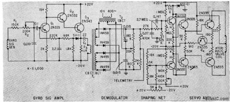
Identical channels amplify, demodulate, and shape gyro signal to feed direct-coupled differential servo amplifier whose output differential cur rent goes to dual-coil hydraulic control valve in rocket.-R. E. King and H. Low, Solid-State Guidance For Able-Series Rockets, Electronics, 33:5, p 60-63. (View)
View full Circuit Diagram | Comments | Reading(685)
TWO_PENTODE_MIXER
Published:2009/7/23 23:58:00 Author:Jessie
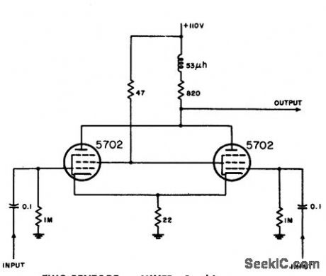
Combines range markers and radar video. Compensated load improves high-frequency response.-NBS, Handbook Preferred Circuits Navy Aeronautical Electronic Equipment, Vol. 1, Electron Tube Circuits, 1963, p N4-4. (View)
View full Circuit Diagram | Comments | Reading(728)
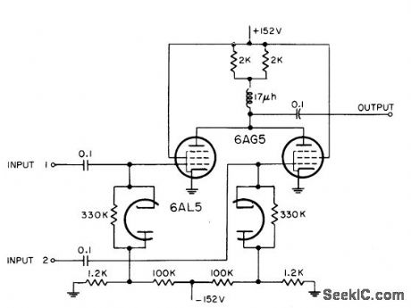
Loopback_tests
Published:2009/7/23 23:57:00 Author:Jessie
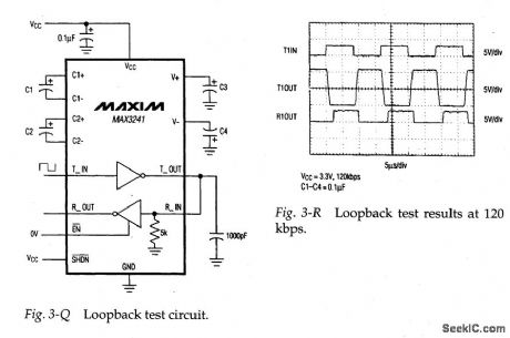
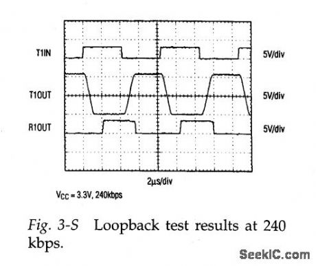
Figure 3-Q shows a loopback test circuit for the MAX3241. Figures 3-R and 3-S show the loopback test results at 120 kbps and 240 kbps, respectively. Notice that the input is applied at the transmitter input, and that both the transmitter output (connected to receiver input) and the receiver output waveforms are monitored. (View)
View full Circuit Diagram | Comments | Reading(937)
TWO_PENTODE_RADAR_AND_IFF_MIXER
Published:2009/7/23 23:57:00 Author:Jessie
Each grid is clamped by diode to establish base line of positive input pulse at -1.8 v.-NBS, Handbook Preferred Circuits Navy Aeronautical Electronic Equipment, Vol. 1, Electron Tube Circuits, 1963, p N4-5. (View)
View full Circuit Diagram | Comments | Reading(723)
RADAR_AND_BEACON_MIXER
Published:2009/7/23 23:56:00 Author:Jessie
Two pentodes combine two inputs into single output.-NBS, Handbook Preferred Circuits Navy Aeronautical Electronic Equipment, Vol. 1, Electron Tube Circuits, 1963, p N4-5. (View)
View full Circuit Diagram | Comments | Reading(733)
STEREO_MULTIPLEXER
Published:2009/7/24 3:15:00 Author:Jessie
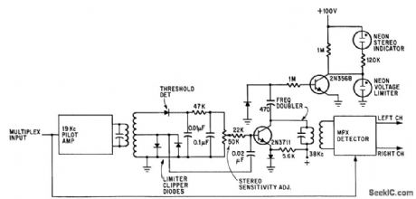
F-m retention is monaural when 19-kc multiplex input is absent or below acceptable power level. Rectification of 19-kc signal provides turn-on voltage to frequency doubler, for stereo.-S. Messin and T. E. Nawalinski, A Solid Stale Stereo Set Built in Modules, Electronics, 38:16, p 88-92. (View)
View full Circuit Diagram | Comments | Reading(673)
FET_SIEREO_FM_TUNER
Published:2009/7/24 3:14:00 Author:Jessie
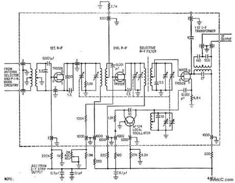
Uses four tuned r-f circuits, two in high-Q highly selective band. pass filter, plus two fet r-f stages in addition to fet mixer and local oscillator. Agc voltage for the two gain-controlled fet r-f stages is derived front fourth i-f stage, which also drives narrow-band meter amplifier.-F. L. Mergner, P-i-n Diode and FET's Improve F-M Reception, Electronics, 39:17, p 114-1 18. (View)
View full Circuit Diagram | Comments | Reading(1514)
300-MHz_complementary_amplifier_56-V_supply
Published:2009/7/24 2:33:00 Author:Jessie
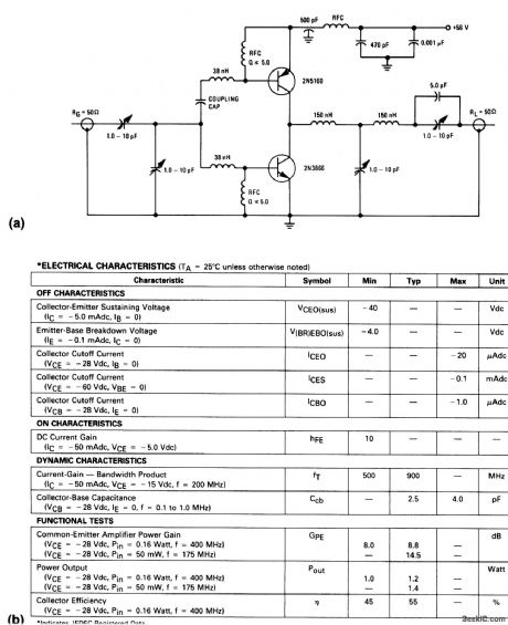
The electrical characteristics for the 2N5160 and 2N3866 shown in this circuit are given in Fig.2-23B and 2-13B,respectively. (View)
View full Circuit Diagram | Comments | Reading(1238)
WELD_TEMPERATURE_CONTROL
Published:2009/7/24 2:29:00 Author:Jessie
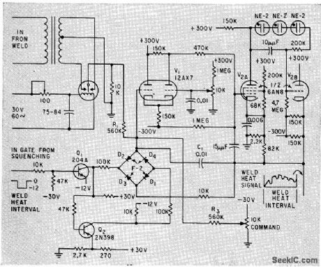
Welding voltage passes through transformer for synchronous rectification to give signal for operational amplifier V1-V2. Output, which is integral of difference between command voltage and resistive input voltage, is used to provide correct, fusion temperature under varied welding conditions.-G. R. Archer, Feedback and NOR Logic Yield Sound Spot Welds, Electronics, 33:8, p 48-51. (View)
View full Circuit Diagram | Comments | Reading(669)
DEMODULATOR_WITH_CARRIER_DETECT
Published:2009/7/3 1:56:00 Author:May
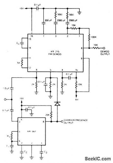
Exar XR-567 PLL system is used with XR-215 FM demodulator to detect presence of carrier signal in narrow-band FM demodulation applications where bandwidth is Iessthan 10% of carrierfrequency. Output of XR-567 is used to turn off FM demodulator when no carrier is present, giving squelch action. Circuit will detect presence of carrier up to 500 kHz.- Phase-Locked Loop Data Book, Exar Integrated Systems, Sunnyvale, CA, 1978, p 41-48. (View)
View full Circuit Diagram | Comments | Reading(1267)
HIGH_GAIN_D_C_PREAMP_FOR_VTVM
Published:2009/7/24 1:49:00 Author:Jessie
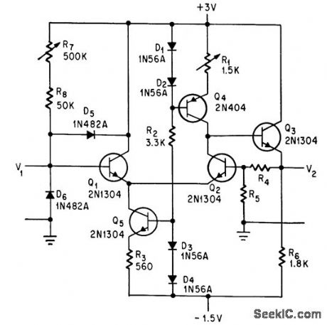
Use of current source as load resistor of Q2 minmizes battery supply effect on zero selling. Additional current source Q5-R3-D3-D4 serves in place of common-emitter resistance for Q1-Q2 to reduce sensitivity to negative supply voltage excursions and boost open-circuit gab above 300. Preamp will extend 1.5-v range down to 500, 150, and 50 my full-scale for voltage measurements in semiconductor circuits without damaging transistors.-A. K. Scidmore, Low-Cost Emitter-Follower Extends Voltmeter's Range, Electronics, 39;3, p 87. (View)
View full Circuit Diagram | Comments | Reading(750)
Typical_RS_485_RS422_network
Published:2009/7/24 1:45:00 Author:Jessie

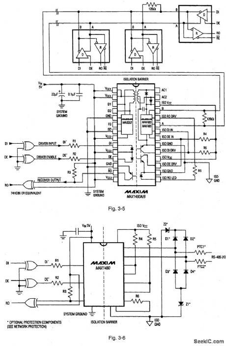
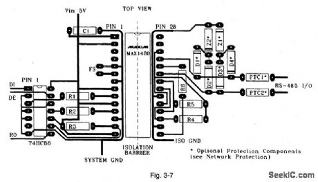
Figure 3-5 shows the MAX1480A/B connected in a typical RS-485/RS422 network. Figures 3-6 and 3-7 show the layout schematic and PC layout. To minimize reflections, terminate the line at both ends with its characteristic impedance, and keep the stub lengths off the main line as short as possible. The slew-rate-limited MAX1408B is more tolerant of imperfect termination and stubs off the main line. MAXIM NEW RELEASES DATA Book, 1995, P. 2-19, 2-21.
(View)
View full Circuit Diagram | Comments | Reading(2692)
| Pages:59/126 At 204142434445464748495051525354555657585960Under 20 |
Circuit Categories
power supply circuit
Amplifier Circuit
Basic Circuit
LED and Light Circuit
Sensor Circuit
Signal Processing
Electrical Equipment Circuit
Control Circuit
Remote Control Circuit
A/D-D/A Converter Circuit
Audio Circuit
Measuring and Test Circuit
Communication Circuit
Computer-Related Circuit
555 Circuit
Automotive Circuit
Repairing Circuit