
Circuit Diagram
Index 1061
Precision_current_monitor
Published:2009/7/23 21:30:00 Author:Jessie

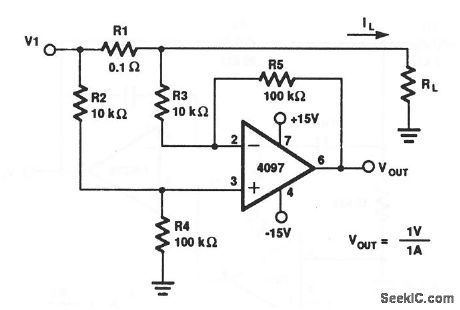
This circuit produces an output voltage that is proportional to the current that is applied to the load RL. (View)
View full Circuit Diagram | Comments | Reading(772)
Low_noise_wide_bandwidth_ampliffer
Published:2009/7/23 21:30:00 Author:Jessie
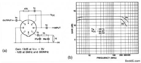
Figure 2-6A shows an SL560 used as a wide-bandwidth amplifier.Figure 2-6B shows the bypical frequency response. (View)
View full Circuit Diagram | Comments | Reading(662)
REGULATED_DIVIDER_FOR_±5V
Published:2009/7/6 2:10:00 Author:May
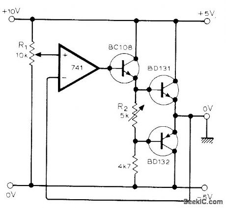
Used at output of adjustable regulated power supply providing up to 15 V, to give lower positive and negative voltages that remain steady despitechanges in load current To get +5 V and -5V from +10 V, set R1 at midposition and adjust R2 for 20 mA through output transistors,Uses 741 opamp.-C.H. Banthorpe、 Voltage Divider, Wireless world, Doc 1976,p41 (View)
View full Circuit Diagram | Comments | Reading(1682)
AFC_FOR_F_M_TUNER
Published:2009/7/23 21:43:00 Author:Jessie
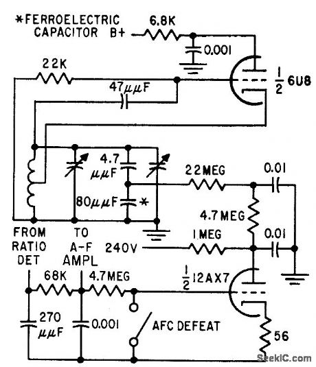
Obtained by amplifying change in output from ratio detector as caused by local oscillator drift, and applying resulting error signal to voltage-tunable ferroelectric capacitor in local oscillator through d-c amplifier,-T. W. Butler, Jr., Ferroelectrics Tune Electronic Circuits, Electronics, 32:3, p 52-55. (View)
View full Circuit Diagram | Comments | Reading(706)
TV_AUDIO_AMPLIFIER
Published:2009/7/6 2:10:00 Author:May
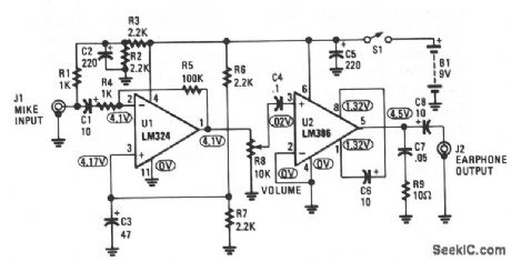
The amplifier picks up the TV's audio output signal and amplifies it to drive a set of earphones for private listening. It is built around an LM324 quad op amp and an LM386 low-power audio amplifier. The circuit uses an inexpensive electret microphone element as the pick-up and a set of earphones as the output device. (View)
View full Circuit Diagram | Comments | Reading(3579)
COUNTER_DRIVE_FOR_WWVB
Published:2009/7/6 2:09:00 Author:May
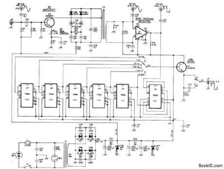
Uses LM311 as true zero-crossing detector for 60-kHz carrier of NBS standard-frequency station at Boulder, Colorado. Resulting square wave is fed to chain of 7490 dividers whose outputs are selected by S2 to serve as gate for frequency counter.T1 is 24-V 500-mA power transformer, and T2 is 40-kHz cupcore slugtuned RF transformer as used in many TV remote controls. Primary inductance (7.5-46 mH) of T2 is tapped at 0.5 mH;secondary is 20 pH. Article also gives circuit of preamp that can be built into 60-kHz loop antenna to build up signal strength to 0.4 V as re quired for input to processor.-H. Isenring, WWVB Signal Processor, Ham Radio, March 1976, p 28-34.
(View)
View full Circuit Diagram | Comments | Reading(2376)
4_bit_D_A_converter_with_microprocessor_interface
Published:2009/7/23 21:43:00 Author:Jessie
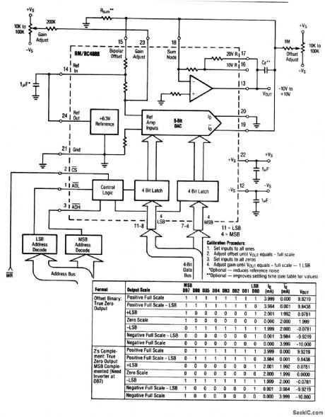
This circuit uses a DAC-4888 and a few external components to form a D/A converter with microprocessor interface (4-bit data bus). The output is + 10 V to -10 V with complementary binary input (all zeros equal full scale). (View)
View full Circuit Diagram | Comments | Reading(845)
FREQUENCY_BOUNDARY_DETECTOR
Published:2009/7/6 2:09:00 Author:May
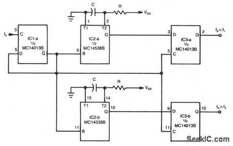
The circuit can be used to tell whether or not an input signal is within a certain frequency range. The device consists of three ICs, a dual monostable multivibrator, and two dual D-type flip-flops. The signal whose frequency is in question is fed to the clock input of one of the flip-flops. The Q output of that flip-f1op (IC1a) is cross coupled to its data input so that it acts like a divide-by-two counter. The trailing edge of the Q output is used to trigger the one shots formed by IC2. The upper- and lower-frequency boundaries are determined by the two sections of IC2 ; the dual precision monostable multivibrator and their external rc networks. The upper-frequency boundary, f1, is set by the output of IC2a, and the lower-frequency boundary, f2, is set by the output of IC2b.
The frequency of the input to the circuit can be anywhere from dc to 100 kHz. The states of the out-puts of IC2, which determine the upper- and lower-frequency boundaries, are latched by IC3a and IC3b respectively. The output of IC3a will be high only when the input frequency is less than that of the output of IC2a, f1 The output of IC3b will be high only when the frequency of the input is greater than that of the output of IC2b, f2. (View)
View full Circuit Diagram | Comments | Reading(944)
CAR_RADIO_WITH_CAPACITIVE_DIODE_TUNING_AND_ELECTRONIC_MW_LW_SWITCHING
Published:2009/7/6 2:09:00 Author:May
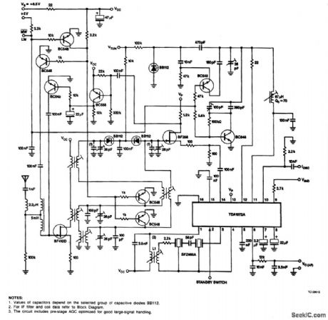
View full Circuit Diagram | Comments | Reading(1604)
EIGHT_COMMAND_TRANSMITTER
Published:2009/7/23 21:43:00 Author:Jessie
Two lone channels can be transmitted simultaneously. Operates at 27 Mc with 0.25.w output, for controlling model tank-R. A. Baker, Radio-Controlled Tank for Realistic Combat Training, Electronics, 33:45, p 55-57. (View)
View full Circuit Diagram | Comments | Reading(1105)
DUAL__52_V_AND___15_V
Published:2009/7/6 2:08:00 Author:May


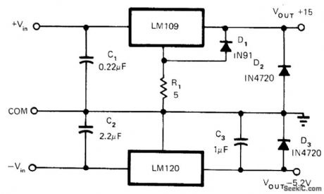
Output voltages are equal to preset values of regulator ICs in basic arrangement shown. R1 and D1 ensure startup of LM109 when common load exists across sup-plies. D1 should be germanium or Schottky hav-ing forward voltage drop of 0.4V or less at 50 mA. D2 and D3 protect against polarity reversal of output during overloads.-C. T. Nelson, Power Distribution and Regulation Can Be Simple, Cheap and Rugged, EDNMagazine, Feb, 20, 1973, p 52-58. (View)
View full Circuit Diagram | Comments | Reading(674)
SPEAKER_AMPLIFIER_FOR_HAND_HELD_TRANSCEIVERS
Published:2009/7/6 2:08:00 Author:May
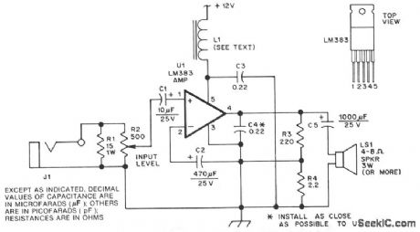
The LM383 is an audio-power amplifier that is capable of producing up to 8W of audio output. R1 is essentially a load resistor for the hand-held transceiver's audio output. R2 can be composed of two fixed resistors in a 10:1 divider arrangement, but using a potentiometer makes it easy to set the amplifier's maximum gain. When powered from a vehicle's electrical system, the amplifier's +12V power source requires filter L1 to eimtnate alternator whine. The LM383 can be mounted directly on the heatsink because the mounting tab is at ground potential. (View)
View full Circuit Diagram | Comments | Reading(892)
Basic_comparator_with_hysteresis
Published:2009/7/23 21:43:00 Author:Jessie
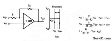
This circuit uses one section of a 3403 op amp as a comparator (without the use of an IC comparator). (View)
View full Circuit Diagram | Comments | Reading(946)
25_250_MHz_PRESCALER
Published:2009/7/6 2:08:00 Author:May
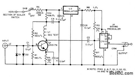
Based on use of Fairchild 95H90 decade counter, with preamp Q1 and associated components selected for 25-250 MHz range. 1N914N diodes prevent over-loading of input. Voltage regulator is LM340T-5, L1 is 8 tums No. 28 wound on body of 1000-ohm or larger 1/2-W resistor, with ends soldered to resistor leads. Quarter.wave whip antenna at inputwill pick up adequate signal from 1-W 146-MHz transceiver hand-held 6-10 feet away.Counter provides division by 10.-R. D. Shriner, Prescaler Updates the DVM/Frequency Counter, QST, Sept. 1978, p 22-24 and 37. (View)
View full Circuit Diagram | Comments | Reading(3212)
SINGLE_CONVERSION_SYNTHESIZER
Published:2009/7/6 2:07:00 Author:May
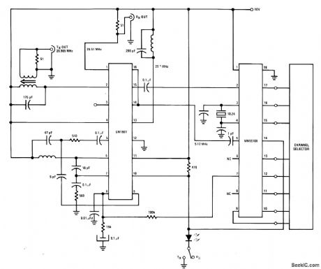
Used in single-conversion CB transceiver in whichVCO operates at channel frequency during transmit and 455 kHz below channel frequency during receive. 5.120 MHz is quintupled to 25.600 MHz to mix and provide input to programmable divider.-L.Sample,A Linear CB Synthesizer, IEEE Transactions on Consumer Electronics Aug,1977、p 200-206 (View)
View full Circuit Diagram | Comments | Reading(778)
Power_supply_monitor_with_reset
Published:2009/7/23 21:40:00 Author:Jessie
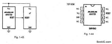
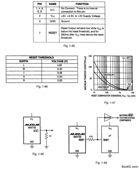
Figures 1-43, 1-44, and 1-45 show a typical application circuit, pin configuration, and pin descriptions, respectively, for the MAX709, The IC provides a system reset during power up, power down and brownout conditions. When VCC falls below the reset threshold (Fig. 1-46), RESET becomes low and holds the microprocessor for 140 ms (minimum) after VCC rises above the threshold. The RESET output is guaranteed to be in the correct state with VCC down to 1 V. The IC is relatively immune to short-duration negative-going VCC transients (glitches), as shown in Fig. 1-47. Figure 1-48 shows the addition of R1 when the RESET output must be valid down to 0 V. The value of R1 should be about 100 kΩ, but it is not critical. Figure 1-49 shows the circuit for interfacing to microprocessors with bidirection reset pins (such as the Motorola 68HC11 series). MAXIM NEW RELEASES DATA BOOK, 1994, P. 5-67, 5-70, 5-71. (View)
View full Circuit Diagram | Comments | Reading(702)
+15_V_WITH_DIFFERENTIAL_AMPLIFIER
Published:2009/7/6 2:07:00 Author:May
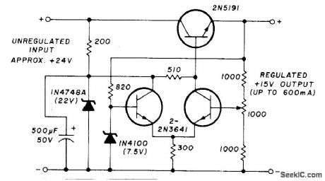
Series regulator uses differential amplifiel as controlcircuit in which one side is referenced to zener and other to fraction of output voltage Second zener provides coarse regulated voltage to differential pair.-H.Olson、Power-Supply Servicing Ham Radio,Nov.1976、p44-50 (View)
View full Circuit Diagram | Comments | Reading(1950)
IMPROVED_PREAMP
Published:2009/7/6 2:04:00 Author:May
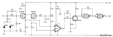
Replaces inefficient input circuit of inexpensive frequency counter, to ensure accurate counting from DC to over 60 MHz Circuit brings input signal waveform to TEL level of 3.5 V P-P while providing required perfect square waves down to lowest-frequency input signal. Input circuit is balanced FET source-follower having extremely high input impedance. Back-to-back diodes provide overload protection. Input stage drives 733 differential video amplifier having 100-MHz band-width and gain of 400. 2N709 switching transistor squares preamp signal for TTL translator using two sections of 74H00 high-speed quad NAND gate. Circuit requires dualpolarity sup ply delivering at least 63 mA; regulation is optionaL-G. Beltrami, High-Impedance Preamp and Pulse Shaper for Frequency Counters, Ham Radio, Feb. 1978, p 47-49.
(View)
View full Circuit Diagram | Comments | Reading(5311)
3_TRANSISTOR_UHF_TUNER
Published:2009/7/23 21:40:00 Author:Jessie
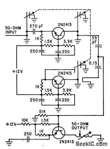
Conversion gain is up to 9 db and noise figure around 8 db, with drain of 18 ma at 12 v.-Transistors Provide Gain in TV Tuner, Electronics, 35:26,p 25. (View)
View full Circuit Diagram | Comments | Reading(1379)
VOLTAGE_CONTROLLED_RAMP_GENERATOR
Published:2009/7/6 2:03:00 Author:May
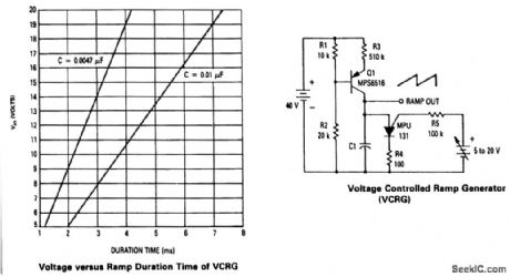
Circuit NotesThe current source formed by Q1 in conjunction with capacitor C1 set the duration time of the ramp. As the positive dc voltage at the gate is changed, the peak point firing voltage of the PUT is changed, which changes the duration time, i.e., increasing the supply voltage increases the peak point firing voltage causing the duration time to increase. (View)
View full Circuit Diagram | Comments | Reading(943)
| Pages:1061/2234 At 2010611062106310641065106610671068106910701071107210731074107510761077107810791080Under 20 |
Circuit Categories
power supply circuit
Amplifier Circuit
Basic Circuit
LED and Light Circuit
Sensor Circuit
Signal Processing
Electrical Equipment Circuit
Control Circuit
Remote Control Circuit
A/D-D/A Converter Circuit
Audio Circuit
Measuring and Test Circuit
Communication Circuit
Computer-Related Circuit
555 Circuit
Automotive Circuit
Repairing Circuit