
Circuit Diagram
Index 1073
Parallel High-Speed Current Driver Circuit Composed Of OPA660
Published:2011/7/30 19:29:00 Author:Robert | Keyword: Parallel, High-Speed, Current, Driver
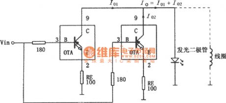
The picture shows the parallel high-speed current driver circuit. The input signal Vin is added to the OPA660 device's equivalent special transistor OTA's base port B (pin 3) through a 180Ω resistor. Two collector ports are connected directly (pin 8) and also connected with the load. They are also supply current to the load. So the current through the load would be twice than a single OTA's current. The OPA660's OTA's maximum output current is ±15mA, but the parallel circuit could provide maximum output current of ±30mA. So when need more current it could take more OPA660 operational amplifiers to be parallel to get the load current needed. The input port (B polar) is connected external 180Ω resistor, which could have the function of current limiting and avoid the self-oscillation of the amplifier and reduce the the peak cases of frequency characteristic. (View)
View full Circuit Diagram | Comments | Reading(735)
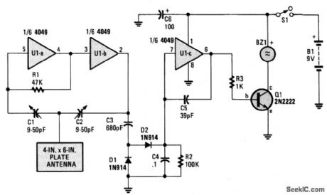
PROXIMITY_ALARM
Published:2009/7/5 23:08:00 Author:May
Circuit Notes
Inverters U1a and U1b are connected in a simple RC oscillator circuit. The frequency is determined by the values of R1, C1, C2, and the intemal characteristics of the integrated circuit. As long as, the circuit is oscillating, a positive dc voltage is developed at the output of the voltage-coupler circuit: C3, D1, D2 and C4. The dc voltage is applied to the input of Ulc-the third inverter amplifier-keeping its output in a low state, which keeps Q1 turned off so that no sound is produced by BZ1. With C1 and C2 adjusted to the most sensitive point, the pickup plate will detect a hand 3 to 5-inches away and sound an alert.Set C1 and C2 to approximately one-half of their maximum value and apply power to the circuit. The circuit should oscillate and no sound should be heard. Using a non-metallic screwdriver, carefully adjust C1 and C2, one at a time, to a lower value until the circuit just ceases oscillation: Buzzer BZ1 should sound off. Back off either C1 or C2 just a smidgen until the oscillator starts up again-that is the most sensitive setting of the circuit. (View)
View full Circuit Diagram | Comments | Reading(0)
PEAK_DETECTOR
Published:2009/7/5 23:07:00 Author:May
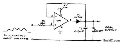
The comparator will charge C1 until the voltage across the capacitor equals the mputvoltage. If subsequent utput vo⒒age exceeds that stored In C1,the comparator voltagewill go high and charge C1 to new higher peak voltage (View)
View full Circuit Diagram | Comments | Reading(0)
DEMONSTRATION_FLIP_FLOP
Published:2009/7/5 23:07:00 Author:May
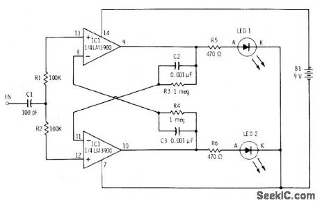
Two sections of LM3900 quad opamp form bistable MVBR for flip-flop having two stable states. When input is grounded momentarily, output of one of opamps swings completely on and turns other opamp off. LED indicates which opamp is on at any particular time. Next grounding of input re verses conditions. Ideal for classroom demonstrations.-F. M. Mims, Integrated Circuit Projects, Vol. 5, Radio Shack, Fort Worth, TX, 1977, 2nd Ed., p 30-37. (View)
View full Circuit Diagram | Comments | Reading(2487)
POSITIVE_PEAK_DETECTOR
Published:2009/7/5 23:07:00 Author:May
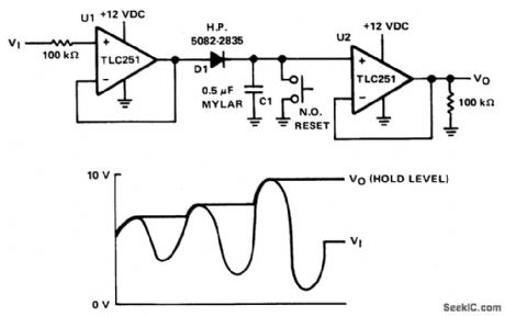
The purpose of the circuit is to hold the peak of the input voltage on capacitor C1, and read the value, VO, at the output of U2. Op amps UI and U2 are connected as voltage followers. When a signal is applied to VI, C1 will charge to this same voltage through diode D1. This positive peak voltage on C1 will maintain VO at this level until the ca-pacitor is reset (shorted). Of course, higher positive peaks will raise this level while lower power peaks will be ignored. C1 can be reset manually with a switch, or electronically with an FET that is normally off. The capacitor specified for C1 should have low leakage and low dielectric absorption. Diode D1 should also have low leakage.
Peak values of negative polarity signals may be detected by reversing D1. (View)
View full Circuit Diagram | Comments | Reading(0)
SCOPE_CALIBRATOR
Published:2009/7/5 23:05:00 Author:May
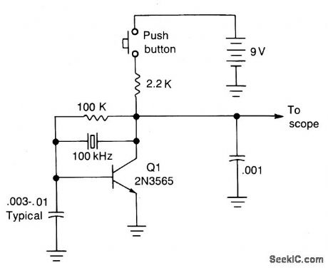
The calibrator operates on exactly 100 kHz providing a reference for calibrating the variable time base oscillator of general purpose scopes. For example, if the scope is set so that one cycle of the signal fills exactly 10 graticule divisions then each division represents 1 MHz, or 1 microsecond. If the scope is adjusted for 10 cycles on 10 graticule divisions. (1 cycle per division) then each division represents 100 kHz or 10 microsecends. (View)
View full Circuit Diagram | Comments | Reading(2232)
NEGATlVE_RESISTANCE_LED_OSCILLATOR
Published:2009/7/5 23:04:00 Author:May
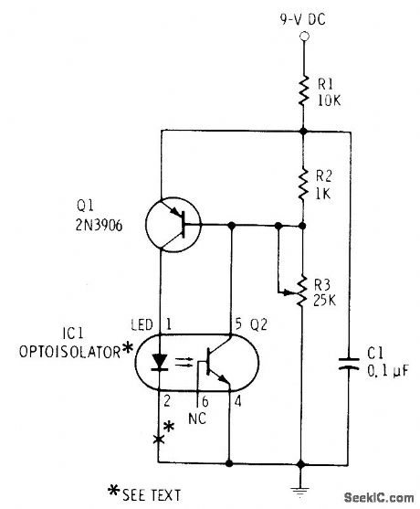
Covers frequency range of about 3.2-8 kHz with values shown. WilI drive Ioudspeaker inserted at point X. For lower frequency (range of 120-1800 Hz) and Iouder sound, change C1 to 1 μF.Negative-resistance portion of circuit indudes Q1, Q2, LED, R2, and R3. Optoisolator can be MCT-2 or equivalent.-F. M, Mims, Electronic Circuitbook 5: LED Projects, Howard W. Sams, Indianapolis, IN, 1976, p 26-29. (View)
View full Circuit Diagram | Comments | Reading(958)
FET_DUAL_TRACE_SCOPE_SWITCH
Published:2009/7/5 23:04:00 Author:May
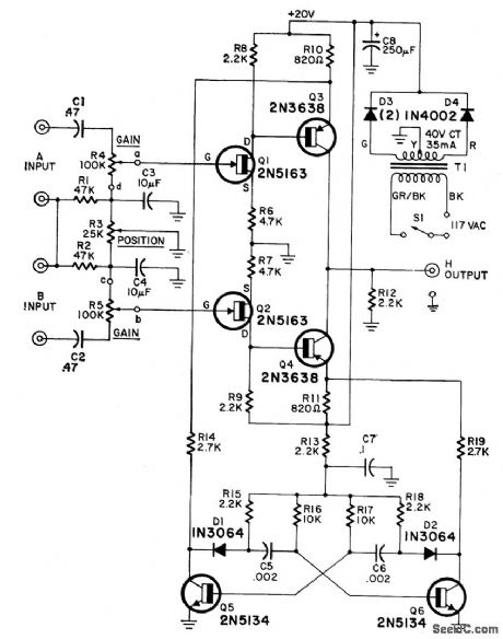
The switcher output goes to the single vertical input of the scope,and a sync line from one of the Inputs is taken to the scope's external-Sync Input.Frequency response of the input amplifiers is 300 kHz over the range of the gain controls.With the gain controls wide open so no attenuatjon of the signal takes place,the frequency response is up to 1 MHz (View)
View full Circuit Diagram | Comments | Reading(1170)
1_Hz_AUTO_FLASHER
Published:2009/7/5 23:03:00 Author:May
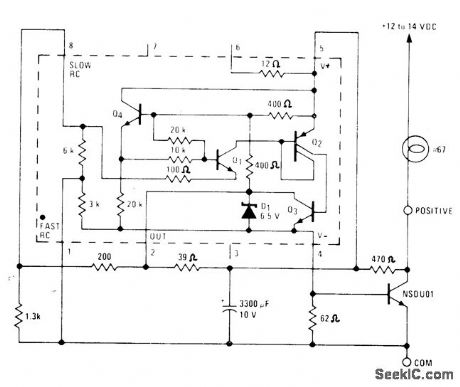


Lamp drawing nominal 600 mA is flashed at 1 Hz by National LM3909 flasher IC operating from 12-V automotive batterv. Use of 3300-μF capacitor makes flasher IC immune to supply spikes and provides means of limiting IC supply voltage to about 7 V.-P.Lefferts, Power-Miser Flasher IC Has Many Novel Applieations, EDN Magazine, March 20, 1976, p 59-66.
(View)
View full Circuit Diagram | Comments | Reading(1072)
SEQUENTIAL_SWITCHING_OF_LOADS
Published:2009/7/5 23:01:00 Author:May
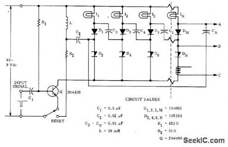
Ring counter using four-layer diodes DN provides sequential switching of loads under control of input pulse-train signal. Indicator lamps are shown, but any load from 15 to 200 mA can be switched. After power is applied, reset switch must be pressed to establish current through L.When switch is released, this current fiows through C2 and breaks down D2, allowing current to flow through first lamp I1. Input pulse to transistol Q (normally held off by current through R1)turns Q off and removes power from diode circuits, thus turning I1 and D2 off. At end of input pulse, a comes on and restores power to diode circuits, but all loads will be turned off.Voltage on C3 now adds to 6 V normally across D4, making D4 break down and turn on I2. Next input pulse will breakdown D6 in same manner.Output signals may be picked up as negative pulses at A or B or by current-sensing at C if required for controlling larger loads,-J. Bliss and D. Zinder, 4-Layer and Current-Limiter Diodes Reduce Circuit Cost and Comptexity, Motorola, Phoenix, AZ, 1974, AN-221, p 5.
(View)
View full Circuit Diagram | Comments | Reading(821)
ANALOG_MULTIPLEXER_CONVERTS_SINGLE_TRACE_SCOPE_TO_FOUR_TRACE
Published:2009/7/5 23:01:00 Author:May
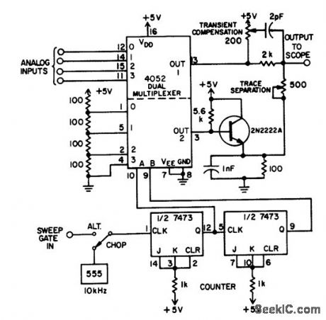
This adapter circuit, based on a dual four-channel analog multiplexer handles digital signals to at least 1 MHz, and analog signals at least through the audio range. The dual multiplexer's upper half selects one input for display. The lower half generates a staircase to offset the baselines of each channel, keeping them separate on the screen. The emitterfollower buffers the staircase, which is then summed with the selected signal. A two-bit binary counter addresses the CMOS 4052 multiplexer. (View)
View full Circuit Diagram | Comments | Reading(3309)
ZENER_CONTROLS_BRIDGE
Published:2009/7/5 23:00:00 Author:May
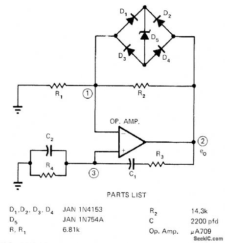
Amplitude of 10.5-kHz Wien-bridge oscillator outputis main-tained symmetrical above ground by using single zener with diode bridge,As output e0 approaches soft knee threshold of conduction for zener.its impedance decreases and shunts R2,This violates oscillator requirement that R2=2R1. so output begins decreasing sinusoidally. As swing decreases, gain increases until e0 reaches negative threshold. Signal then reverses and again starts going positive.-W. B Crittenden and E. J. Owings, Jr., Zener-Diode Controls Wien-Bridge Oscillator, EDN Magazine. Aug. 1. 1972. p 57-58. (View)
View full Circuit Diagram | Comments | Reading(1375)
TONE_PROBE_FOR_TESTING_DIGITAL_ICs
Published:2009/7/5 23:00:00 Author:May
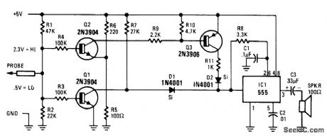
Circuit Notes
The tone probe uses sound to tell the status of the signal being probed. The probe's input circuit senses the condition of the signal and produces either a low-pitched tone for low-level signals (less than 0.8 V) or a high-pitched tone for high-level signals (greater than 2 V). (View)
View full Circuit Diagram | Comments | Reading(0)
Multi-Stage Output Delay Circuit
Published:2011/7/27 8:41:00 Author:Robert | Keyword: Multi-Stage, Output, Delay
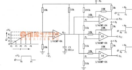
The picture shows the multi-stage output delay circuit. In the circuit it uses the operational amplifier as the comparator. When the operational amplifier A1's in-phase input port is added the +VE voltage, the voltage VC1 on the operational amplifier A2, A3, A4's in-phase input ports would increase by following the law of exponential curve. The operational amplifier's out-phase input port is added the voltage provided by the voltage classification divider. So each operational amplifier's input would reverse each output signal separately at the time of t1, t2, t3 during Vc1 is from zero to +VB(power voltage). That achieves the purpose of VA1, VA2, VA3's delaying progressively. It should be noted that this circuit uses dual power supplies which is positive power +VE, +VB and negative power -VB. (View)
View full Circuit Diagram | Comments | Reading(814)
Electric Blanket And Rice Cooker Timer Circuit
Published:2011/7/28 6:55:00 Author:Robert | Keyword: Electric Blanket, Rice Cooker, Timer
The picture shows the electric blanket and rice cooker timer circuit. This circuit's timing time could be set from 1 second to more than 10 hours. In the picture, C1 is timing element. When the power supply is connected, pressing the switch AN1, the C1 would be charging to DC 28V. The comparator A would output high voltage level and the transistor VT would be connected, the relay J would be powered up and have actions. The J1-1 would be conncted and the power would be self-locked. The J1-2 would be disconnected. C1 would discharge to the high-resistance input port. When the C1's voltage is decreased and lower than the A's out-phase input port, the A would output low voltage level, the transistor VT would be disconnected, J would lost the power and be released. Then the timing is over until next case that the timing trigger switch AN1 is pressed again. (View)
View full Circuit Diagram | Comments | Reading(3112)
TRANSISTOR_GAIN_AND_LEAKAGE_TESTER
Published:2009/7/23 21:52:00 Author:Jessie
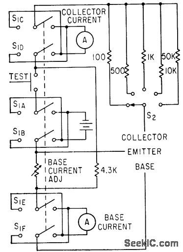
Designed for general testing of production units. Switch S1 changes over from npn to pnp transistors. After controls are set for a specific transistor type, checking involves only noting base current when lest button is, pressed.-F. W. Kear, Simple Test for Transistor Quality, Electronics, 35:39, p 80-81. (View)
View full Circuit Diagram | Comments | Reading(865)
FET_MIXER_FOR_UHF_TV_TUNER
Published:2009/7/23 21:51:00 Author:Jessie
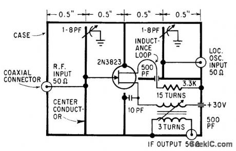
Uses strip transmission lines. Ground-plane conductors divide circuit into three shielded cubicles, for r-f input, local oscillator output, and i-f output.-S. M. Weaver, For a Good Mixer, Add One FET, Electronics, 39:6, p 109-112. (View)
View full Circuit Diagram | Comments | Reading(1013)
Symmetrical_offset_D_A_converter
Published:2009/7/23 21:51:00 Author:Jessie
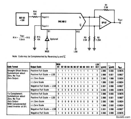
This circuit shows a DAC/op-amp combination that is used to provide symmetrical-offset operation. Full-scale adjustment can be made as shown in Fig.6-39B. (View)
View full Circuit Diagram | Comments | Reading(812)
CAPACITIVELY_TUNED_TUNNEL_DIODE_TUNER_
Published:2009/7/23 21:50:00 Author:Jessie
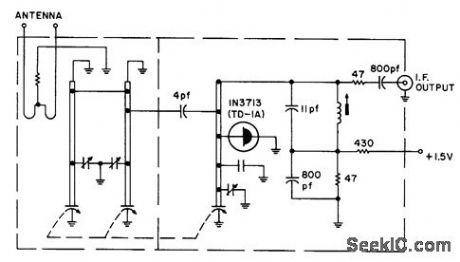
Uses self-oscillating tunnel-diode converter circuit.- Transistor Manual, Seventh Edition, General Electric Co., 1964, p 359. (View)
View full Circuit Diagram | Comments | Reading(731)
CRYOGENIC_CONTACT_TESTER
Published:2009/7/23 21:50:00 Author:Jessie
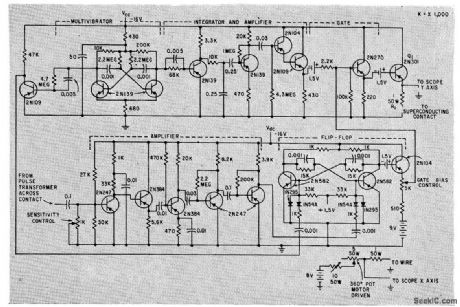
Measures critical current in superconducting contacts during periods shorter than 100 microsec in which such currents can be maintained, and gives oscilloscope display.-J. I. Pankove and R. Drake, Measuring Critical Current in Cryogenic Circuits, Electronics, 33:4, p 52-53. (View)
View full Circuit Diagram | Comments | Reading(735)
| Pages:1073/2234 At 2010611062106310641065106610671068106910701071107210731074107510761077107810791080Under 20 |
Circuit Categories
power supply circuit
Amplifier Circuit
Basic Circuit
LED and Light Circuit
Sensor Circuit
Signal Processing
Electrical Equipment Circuit
Control Circuit
Remote Control Circuit
A/D-D/A Converter Circuit
Audio Circuit
Measuring and Test Circuit
Communication Circuit
Computer-Related Circuit
555 Circuit
Automotive Circuit
Repairing Circuit