
Circuit Diagram
Index 1066
CARRIER_CURRENT_TV_CONTROL
Published:2009/7/23 21:40:00 Author:Jessie
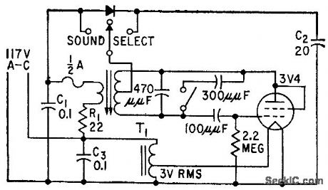
Low-power oscillator provides both unmodulated and 60-cps modulated signals for power-line carrier. current transmission to control receiver in tv set. Unmodulated carrier having preset duration controls channel selection, while modulated carrier controls sound level. System operates on one of four nonadjacent frequencies (52.5, 57.5, 67.5, and 73.5 kc) to ovoid interaction between nearby systems,-J. R. Banker and C. H. Wood, Jr., Line Current Controls Remote Tv Receiver, Electronics, 31:33, p 68-69. (View)
View full Circuit Diagram | Comments | Reading(1224)
4_46_MHz_TUNABLE
Published:2009/7/6 0:57:00 Author:May
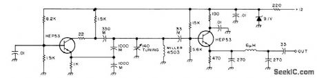
Emitter-follower buffer stage for isolation has low-pass filter for reducing harmonic output and giving better sine-wave output. Oscillator coil should be in shield at least twice coil diameter.-An Accessory VFO-the Easy Way, 73 Magazine, Aug. 1975, p 103 and 106-108. (View)
View full Circuit Diagram | Comments | Reading(888)
High_level_mixer
Published:2009/7/23 21:40:00 Author:Jessie
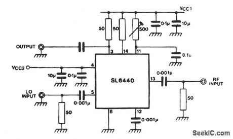
The SL6440,shown is a double-balanced mixer, for use in RF systems up to 150 MHz. External selection of the dc operating conditions is controlled by the resistor connected between pin 11 (bias) and VCC. Conversion gain for single-ended circuit of Fig. 2-10 is equal to: GdB 20 Log56.61+0.0785,RLIp, where Ip is programmed current at pin 11, and RL is dc load resistance. (View)
View full Circuit Diagram | Comments | Reading(1144)
SWITCHED_OVERTONE_CRYSTALS
Published:2009/7/6 0:57:00 Author:May
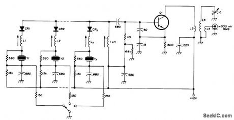
Uses third-overtone crystals between 20 and 80 MHz, with diode switching and with frequency doubling in transistors. L1-Ln ate series resonant with 10 pF at each crystal frequency. L4 is resonant with l0 pF at desired output frequency. L3 and L5 have one-third as many turns as L4. Q1 is 2N918, BF115, HEP709, or equivalent. Diodes are switching types such as BAY67.-U. Rohde, Stable Crystal Oscillators, Ham Radio, June 1975, p 34-37. (View)
View full Circuit Diagram | Comments | Reading(1171)
15_65_MHz_THIRD_OVERTONE
Published:2009/7/6 0:56:00 Author:May
Crystal starting is reliable, and power dissipation of crystal is well below allowable maximum. Q1 is 2N918, 2N3564, 2N5770, BF180, or BF200. L1 resonates at crystal frequency with 22 pF (1μH for 15-30 MHz or 0.5μH for 30-65 MHz). Stability is as good as that of fundamental-frequency oscillator. Set L1 roughly to frequency with no supply voltage by shorting crystal and dipping L1 with grid-dip oscillator. Now apply power and tune L1 close to marked crystal frequency while monitoring output frequency. Remove short and trim to frequency with 3-30 pF trimmer.-R. Harrison, Survey of Crystal Oscillators, Ham Radio, March 1976, p 10-22. (View)
View full Circuit Diagram | Comments | Reading(2122)
283_MHz_THIRD_OVERTONE_TTL
Published:2009/7/6 0:55:00 Author:May
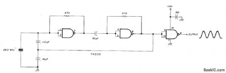
Third-over-tone crystal oscillator uses 74S00 Schottky TTL quad NAND gates acting as oscillator and output buffer to increase output amplitude. Output swing is from about 0.4 to 3.5 V P-P, as required for TTL. No inductors are required.-C. Hall, Overtone Crystal Oscillators Without Inductors, Ham Radio, April 1978, p 50-51. (View)
View full Circuit Diagram | Comments | Reading(1824)
1_kHz_V_FOR_VCO
Published:2009/7/6 0:55:00 Author:May
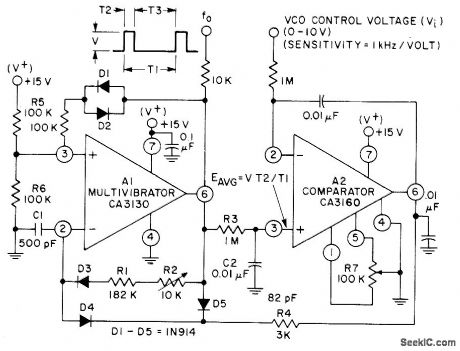
Voltage-contronea oscillator uses CA3130 opamp as MVBR and CA3160 opamp as comparator. Tracking error is about 0.02%, and temperature coefficient is 0.01% per degree C.- Circuit Ideas for RCA Linear ICs, RCA Solid State Division, Somerville, NJ, 1977, p4. (View)
View full Circuit Diagram | Comments | Reading(896)
18_60_MHz_THIRD_OVERTONE
Published:2009/7/6 0:55:00 Author:May
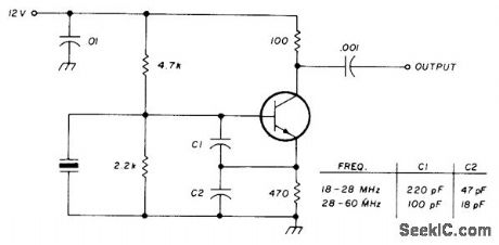
International Crystal OF-1 oscillator for third-overtone crystals requires no inductors. Crystal operates near series resonance, making capacitor unnecessary in series with crystal. With 28.3-MHz third-overtone crystal, circuit delivers 28.3 MHz when C1 is 100 pF and C2 is 18 pF. Using larger values given in table produces oscillation at fundamental of 9.43 MHz.-C. Hall, Overtone Crystal Oscillators Without Inductors, Ham Radio, April 1978, p 50-51. (View)
View full Circuit Diagram | Comments | Reading(2316)
STABLE_35_38_MHz_VFO
Published:2009/7/6 0:54:00 Author:May
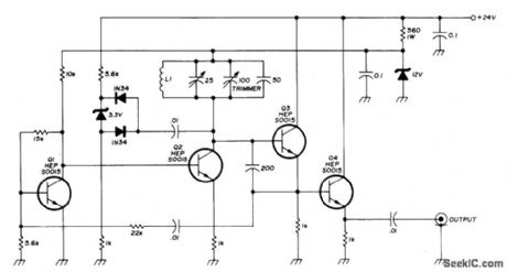
Oscillator Q1-Q2, emitter-follower output Q3, and buffer Q4 provide 5 V P-P into 200-ohm load, with good isolation between oscillator and load Total drift is less than 10 Hz from turn-on, and less than 330 Hz as supply voltage varies between 15 and 30 V. Amplitude stability is within 1 dB over tuning range. Oscillator amplitude is stabilized by two 1N34 diodes and 3.3-V zener. L1 is 25 turns No. 18 closewound on 1.5-in form. –J. Fisk, Circuit sand Techniques, Ham Radio, June 1976, p 48-52. (View)
View full Circuit Diagram | Comments | Reading(957)
10_kHz_SINE_COSlNE
Published:2009/7/6 0:52:00 Author:May
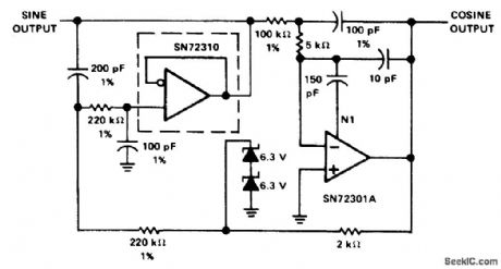
Combination of SN72310 voltage-follower opamp and SN 72301A high-performance opamp gives two outputs differing in phase by 900. Supply is ±18 V.- The Linear and Interface Circuits Data Book for Design Engineers, Texas Instruments, Dallas, TX, 1973, p 4-40. (View)
View full Circuit Diagram | Comments | Reading(723)
160_METER_VFO
Published:2009/7/6 0:52:00 Author:May
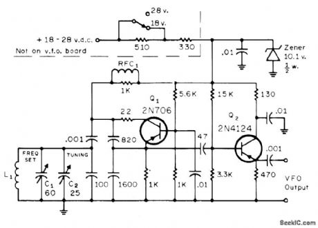
Standard Colpitts oscillator Q1 with emitter-follower Q2 gives dependability and adequate isolation from later stages Zener regulation provides stability even with weak battery Output is about 0.7 VRMS. Low-level parasitic oscillation may occur about 150 kHz below operating frequency but is suppressed by tuned stages following VFO. L1 is 52 turns No. 28 enamel on Amidon T-50-2 toroid. RFC1 is 850μH.-A Weiss, Design Notes on a Moderate Power Solid State Transmitter for 1.8 MHz, CQ, Nov. 1972, p 18-22, 24, 98, 100, and 102. (View)
View full Circuit Diagram | Comments | Reading(1854)
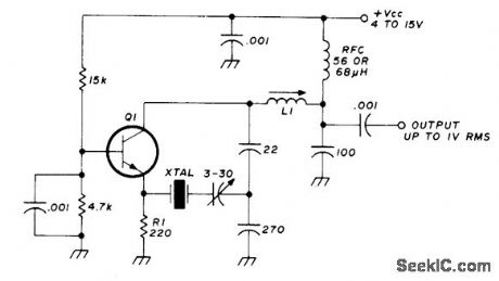
3_20_MHz_CRYSTAL
Published:2009/7/6 0:51:00 Author:May
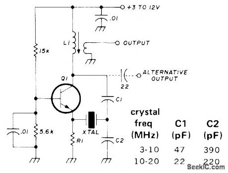
Circuit is series-mode oscillator, but parallel-mode crystals can be used if trimmer in series with crystal is replaced by short-circuit. Adjust feedback by varying ratio of C1 to C2. Use grid-dip oscillator to resonate L1 with C1 when crystal is shorted; then remove short and tune slug of L1 to pull crystal exactly to frequency. R1 should be between 100 and 1000 ohms. The lower its value, the lower the crystal power dissipation and the better is stability. Q1 is 2N918, 2N3564, 2N5770, BF200, SE1001, or equivalent.-R. Harrison, Survey of Crystal Oscillators, Ham Radio, March 1976, p 10-22. (View)
View full Circuit Diagram | Comments | Reading(2329)
SURE_STARTING_CRYSTAL
Published:2009/7/6 0:50:00 Author:May
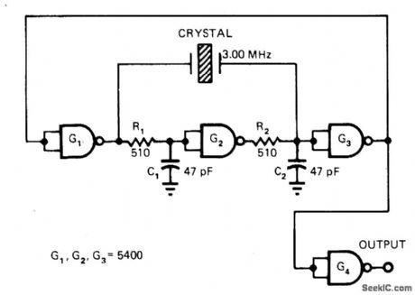
Loop-within-a-loop oscillator design ensures reliable starting without use of critical components Frequency depends on crystal, which can be anywhere in range from 1 to 20 MHz IC can be 54L00 for 1-2 MHz、standard 54H00 for 2-6 MHz, and 54H00 or 54S00 for 6-20 MHz. Temperature stability is adequate for crystal clocks and other digital-system applications.-J. E. Buchanan, Crystal-Oscillator Design Eliminates Start-Up Problems, EDN Magazine, Feb. 20, 1978, p 110. (View)
View full Circuit Diagram | Comments | Reading(980)
LOW_DRIFT_7_MHz_VFO
Published:2009/7/6 0:48:00 Author:May

Low-drift solid-state design for 40-meter band has maximum change of only 25 Hz from cold start to full warm-up at 25℃. After stabilization, maximum hunting is 5 Hz. Drift is minimized by paralleling two or more capacitors in critical parts of circuit. Series-tuned Colpitts oscillator is followed by two buffer stages, with second providing enough amplification for practical amateur work while further improving isolation of oscillator. Low-impedance output network minimizes oscillator pulling from load changes. Article stresses importance of choosing and using components that minimize drift.-D. DeMaw, VFO Design Techniques for Improved Stability, Ham Radio, June 1976, p 10-17. (View)
View full Circuit Diagram | Comments | Reading(2502)
1850_Hz_DIGITAL_IC
Published:2009/7/6 0:46:00 Author:May
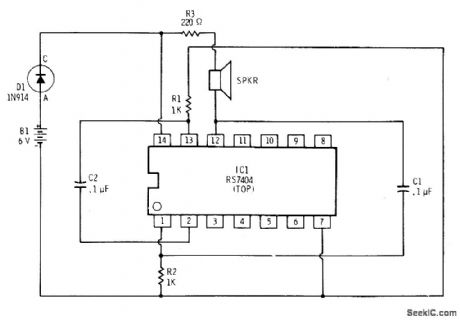
Two sections of RS7404 hex inverter are connected as astable MVBR operating at frequency determined by values used for C1 and C2. Output drives loudspeaker as shown to produce audible tones or can be connected to flash LEDs. D1 reduces battery voltage to 5 V required by 1C. Developed for classroom demonstrations. Circuit produces nearly square waves with amplitude of about 3 V and pulse width of about μ100 pos if used as squarewave generator.-F. M. Mims, Integrated Circuit Projects, Vol. 6. Radio Shack. Fort Worth. TX, 1977, p 64-69. (View)
View full Circuit Diagram | Comments | Reading(816)
100_kHz_WIEN_BRIDGE
Published:2009/7/6 0:46:00 Author:May
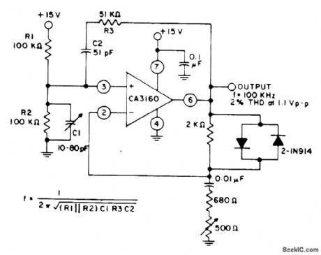
CA3160 opamp in bridge circuit oporates from single 15-V supply. Paralle-connected diodes form gain-setting network that stabilizes output voltage at about 1.1 V. 500-ohm pot is adjusted so oscillator always starts and oscillation is maintained.- Linear Integrated Circuits and MOS/FET's, RCA Solid State Division, Somerville, NJ, 1977, p 271-272. (View)
View full Circuit Diagram | Comments | Reading(1865)
DUAL_FREOUENCY_CRYSTAL
Published:2009/7/6 0:46:00 Author:May
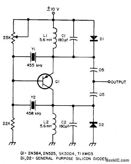
Uses two different crystals, with frequency being changed by reversing supply voltage,Transistor then inverts itself and gain reduces to about 2, which is adequate for oscillator operation Provides two frequencies from single stage with minimum of switching.-Circuits, 73 Magazine, Feb. 1974, p 101. (View)
View full Circuit Diagram | Comments | Reading(989)
IC_CRYSTAL
Published:2009/7/6 0:45:00 Author:May
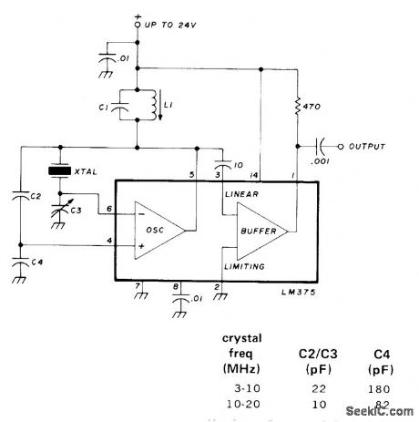
Uses LM375 IC with crystals from 3 to 20 MHz in parallel mode. Will oscillate with only 4-V supply, but output voltage increases with supply voltage, L1 -C1 is resonant at crystal frequency. Adjust L1 only for maximum output, not for trimming frequency. If C3 is 3-30 pF, it can be used to adjust frequency of crystal.-R. Harrison, Survey of Crystal Oscillators, Ham Radio, March 1976, p 10-22. (View)
View full Circuit Diagram | Comments | Reading(1109)
CRYSTAL_SWITCHING_DIODES
Published:2009/7/6 0:44:00 Author:May
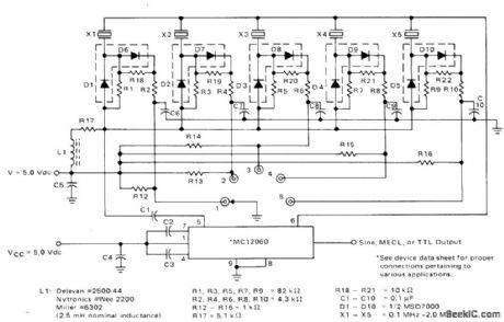
Circuit for Motorola MC12060 crystal oscillator uses diodes as BF switches giving choice of five different crystal frequencies Forward bias is applied to diode associated with desired crystal and reverse bias to diodes for other four crystals. Diode switching eliminates need to run high-frequency signals through mechanical switch, permits control of switching from remote location, and is readily adapted to electronic scanning. Requires only single 5-V supply. Frequency pulling is minimized.-J. Hatchett and R. Janikowski, “Crystal Swtiching Methods for MC12060/MC12062 Oscillator,” Motorola, Phoenix, AZ, 1975, AN-756. (View)
View full Circuit Diagram | Comments | Reading(873)
DAC_current_loop_controller
Published:2009/7/25 5:40:00 Author:Jessie
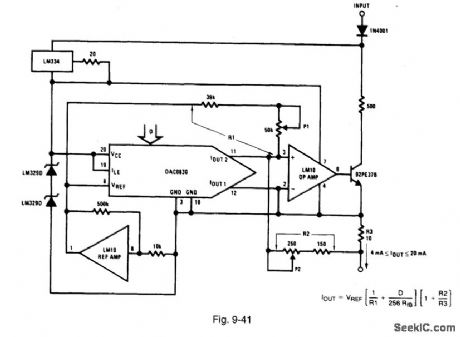
Figure 9-41 shows a DAC0830 connected to provide digital control ofthe standard 3-mA to 20 mA industrial-process current loop. The circuit is two-terminal, and all circuit components (including the DAC) are powered directly from the loop,The output transistor conducts whatever current is necessary to keep the voltage across R3 equal to the voltage across R2.This voltage and therefore the total loop current is directly proportional to the output current from the DAC. The net resistance of R1 is used to set the zero-code loop current to 4 mA and R2 is adjusted to provide the 16-mA output span for a full-scale DAC code. The entire circuit floats by operating whatever ground-reference potential is required for the total loop resistance andloop current,The voltage differential between the input and output terminals mustbe kept in the range of 16 V to 55 V and the digital inputs to the DAC must beelectronically isolated from the ground potential. of the controlling microprocessor.This isolation can best be achieved with opto-isolators.in a non microprocessor system in which the loop-controlling information comes from thumb wheel switches(or a similar mechanical device) the digital input for the DAC can be taken from BCD-to-binary CMOS logic elements (which are ground referenced to the groundpotential of the DAC).The total Supply current requirements of all circuits usedmust (of course) be less than 4 mA and R1 can be adjusted accordingly. NATIONAL SEMICONDUCTOR, APPLICATION NOTE 271. 1994. P. 670. (View)
View full Circuit Diagram | Comments | Reading(927)
| Pages:1066/2234 At 2010611062106310641065106610671068106910701071107210731074107510761077107810791080Under 20 |
Circuit Categories
power supply circuit
Amplifier Circuit
Basic Circuit
LED and Light Circuit
Sensor Circuit
Signal Processing
Electrical Equipment Circuit
Control Circuit
Remote Control Circuit
A/D-D/A Converter Circuit
Audio Circuit
Measuring and Test Circuit
Communication Circuit
Computer-Related Circuit
555 Circuit
Automotive Circuit
Repairing Circuit