
Circuit Diagram
Index 1060
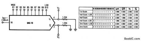
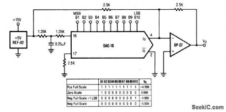
Basic_bipolar_output_DAC
Published:2009/7/23 21:29:00 Author:Jessie
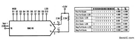
This circuit shows a DAC that is connected for bipolar-output D/A-converter operation. (View)
View full Circuit Diagram | Comments | Reading(841)
Low_noise_preamplifier
Published:2009/7/23 21:29:00 Author:Jessie
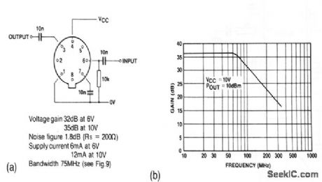
Figure 2-5A shows an SL560 used as a preamplifier.Figure 2-5B shows the typical frequency response. (View)
View full Circuit Diagram | Comments | Reading(748)
500_KC_SCHMITT_TRIGGER
Published:2009/7/23 21:29:00 Author:Jessie
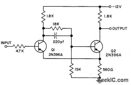
Used for wave form restoration, signal level shifting, squaring, and d-c level detection. Q1 conducts if input is more negative than -5 v. Q2 conducts when input is more positive than -2 v. Operating range is -55 to 71℃.- Transistor Manual, Seventh Edition, General Electric Co., 1964, p 200. (View)
View full Circuit Diagram | Comments | Reading(819)
Analog_multiplier
Published:2009/7/23 21:29:00 Author:Jessie
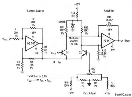

The output of this circuit is equal to input A times input B times 100, using the values shown. (View)
View full Circuit Diagram | Comments | Reading(0)
Low_noise_line_driver
Published:2009/7/23 21:28:00 Author:Jessie
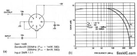
Figure 2-4A shows an SL560 used as a 50-Ω line driver. Figure 2-4B shows the typical frequency response. (View)
View full Circuit Diagram | Comments | Reading(960)
Microprocessor_supervisory_circuit_added_features
Published:2009/7/23 21:28:00 Author:Jessie
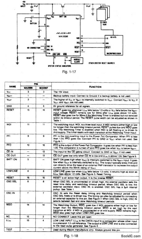
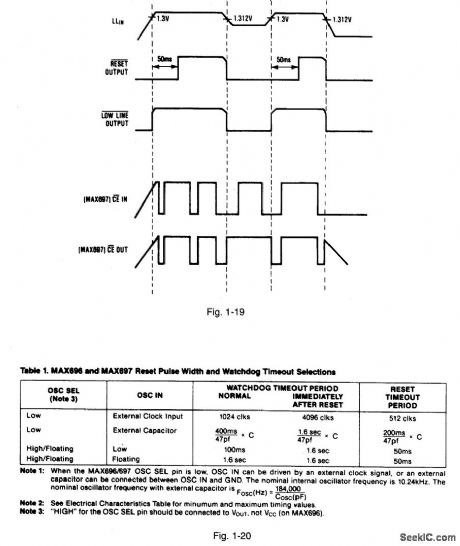
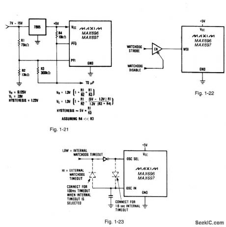
Figures 1-17 and 1-18 show a typical application circuit and pin descriptions, respectively for a MAX696. The IC is similar to that described for Figs. 1-J through 1-N, but with added (or combined) features. Use the equations shown in Fig. 1-M to calculate the values for the resistors at the PFI and LLIN inputs (except use a threshold of 1.3 V, instead of 2.54 V). Figures 1-19, 1-20, 1-21, 1-22, and 1-23 show the reset timing, watchdog and reset timeout selection, calculations and connections for adding hysteresis, circuit for disabling the watchdog under program control, and circuit for selecting watchdog timeout, respectively. Table 1 in Fig. 1-18 refers to Fig. 1-20 in this book. Figure 1 in Fig. 1-18 refers to Fig. 1-17 in this book. Figure 5 in Fig. 1-18 refers to Fig. 1-19 in this book. Figure 7 in Fig. 1-18 refers to Fig. 1-21 in this book. Figure 2 in Fig. 1-18 is an internal function not shown here. MAXIM NEW RELEASES DATA Book, 1992, P. 5-36, 5-37, 5-41, 5-43. (View)
View full Circuit Diagram | Comments | Reading(697)
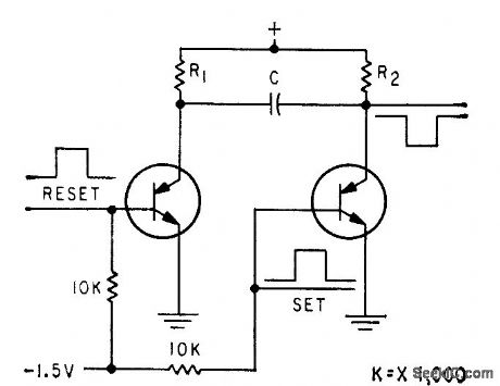
COLLECTOR_TRIGGERED_FLIP_FLOP
Published:2009/7/23 21:28:00 Author:Jessie
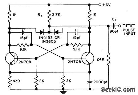
Diodes with basic flip-lop serve as steering circuit,with negative input pulse being used to trigger collectors. Maximum trigger rate exceeds 5 Mc with trigger amplitude from 4 to 12 v.- Transistor Manual, Seventh Edition, General Electric Co., 1964, p 197. (View)
View full Circuit Diagram | Comments | Reading(759)
Low_noise_wideband_amplifier_with_AGC
Published:2009/7/23 21:28:00 Author:Jessie

This circuit combines an SL550 (amplifier with external gain control) and an SL560 (low-noise amplifier) to form a very simple wideband amplifier with AGC. (View)
View full Circuit Diagram | Comments | Reading(897)
Basic_unipolar_negative_reference__DAC
Published:2009/7/23 21:27:00 Author:Jessie
This circuit shows a DAC that is connected for unipolar negative-reference D/A-converter operation. (View)
View full Circuit Diagram | Comments | Reading(558)
Input_amplifier_for_a_4_1_2_digit_voltmeter_
Published:2009/7/23 21:27:00 Author:Jessie
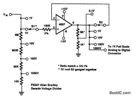
This circuit provides an approximate 10-MΩ input impedance, and can be used with any 1-V full-scale A/D converter. (View)
View full Circuit Diagram | Comments | Reading(769)
Low_cost_supervisory_circuit_with_battery_backup
Published:2009/7/23 21:34:00 Author:Jessie
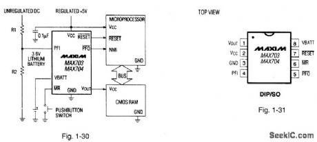
Figures 1-30 and 1-31 show a typical application circuit and pin configurations, respectively, for the MAX703/MAX704. The ICs are similar to that described for Figs. 1-J through 1-M, but with generally lower cost. The ICs have a 200-ms reset pulse width, 200-μA quiescent current, 50-nA quiescent with battery backup, and a 1.25-V threshold detector for power-fail warning, low-battery detection, or for monitoring a power supply voltage other than +5 V. MAXIM HIGH-RELIABILITY DATA Book, 1993, P. 5-29 (View)
View full Circuit Diagram | Comments | Reading(716)
Basic_inverting_amplifier
Published:2009/7/23 21:34:00 Author:Jessie
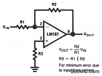
This circuit shows an LM107 that is connected in the classic inverting-amplifier configuration, where VOUT is opposite to VIN (if VIN goes positive, VOUT goes negative, and vice versa). The amplitude of the output depends on the ratio of R1 and R2 (within the limits of the supply voltage), and R3 is selected to equal the parallel resistance of R1 and R2. (View)
View full Circuit Diagram | Comments | Reading(694)
Microprocessor_supervisory_circuit_high_reliability_added_features)
Published:2009/7/23 21:33:00 Author:Jessie
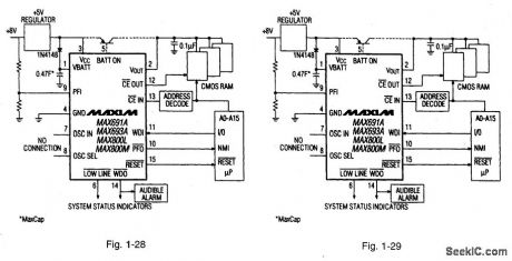
Figures 1-28 and 1-29 show a typical application circuit and pin configurations, respectively, for the MAX691 A /693A /800L / 800M. The ICs are similar to that described for Figs. 1-J through 1-M, but with more reliability and added features.The ICs improve performance with 35-μA supply current, 200-ms typical reset delay on power-up, and 6-ns chip-enable propagation delay. Other features include write protection of CMOS RAM or EEPROM, separate watchdog outputs, battery-backup switchover, and a reset output that is valid with VCC down to 1 V.The MAX691A/MAX800L have a 4.65-V typical reset-threshold. The MAX693A/ MAX800M reset threshold is 4.4V (typical). The MAX800L/MAX800M is guaranteed to deliver power-fail accuracies to 12%. MAXIM HIGH-RELIABILITY DATA Book, 1993, P. 5-19. (View)
View full Circuit Diagram | Comments | Reading(936)
N_STAGE_RING_COUNTER
Published:2009/7/23 21:32:00 Author:Jessie
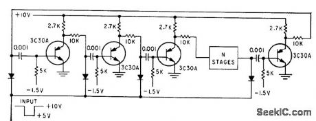
Uses modified memory circuit, in which input pulse turns off all pnpn stages except that following on stage.-J. B. Hangstefer and L.H. Dixon, Jr., Triggered Bistable Semiconductor Circuits, Electronics, 32:35, p 58-60. (View)
View full Circuit Diagram | Comments | Reading(805)
Tracking_positive_and_negative_voltage_references
Published:2009/7/23 21:32:00 Author:Jessie
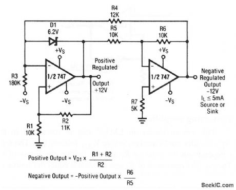
This circuit provides both positive and negative that remain constant, in spite of changes in source voltage or VS. (View)
View full Circuit Diagram | Comments | Reading(684)
Microprocessor_supervisory_circuit_high_reliability
Published:2009/7/23 21:31:00 Author:Jessie
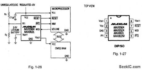
Figures 1-26 and 1-27 show a typical application circuit and pin configurations, respectively, for the MAX690A/MAX802L. The ICs are similar to that described for Figs. 1-J through 1-N, but with added reliability and other reset thresholds. The MAX690A/MAX802L generate a reset pulse when the supply drops below 4.65V, and the MAX692A/MAX802M generate a reset below 4.40 V. The threshold is 1.25V for both power-fail warning and low-battery detection. The reset delay is 200 ms. The watchdog timer has a 1.6-s timeout. Quiescent current is 200μA with normal power and 50nA in battery-backup mode. The power-fail accuracy is ±2% for MAX802L/M. MAXIM HIGH-RELIABILITY DATA Book, 1993, P. 5-17. (View)
View full Circuit Diagram | Comments | Reading(746)
Low_noise_high_gain_amplifier
Published:2009/7/23 21:31:00 Author:Jessie
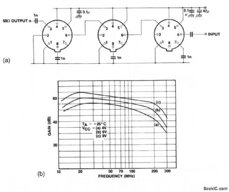
Figure 2-7A shows an SL560 used as a direct-coupled-coupled high-gain amplifier. Figure 2-7B shows the typical frequency response. (View)
View full Circuit Diagram | Comments | Reading(600)
POWER_FLIP_FLOP
Published:2009/7/23 21:31:00 Author:Jessie
Delivers square wave output pulse of 1 amp when pnpn unit is triggered on by low-level positive pulse applied to its base.-J. B. Hangstefer and L. H. Dixon, Jr., Triggered Bistable Semiconductor Circuits, Electronics, 32:35, p 58-60. (View)
View full Circuit Diagram | Comments | Reading(880)
LOW_COST_BASIC_SCHMITT
Published:2009/7/23 21:30:00 Author:Jessie
Developed for use with inexpensive 2N711 germanium pnp mesa switching transistors. Can serve as source of 10-Mc square waves, as pulse restorer, or as general-purpose square wave generator.-P. A. Mclnnis, Low-Cost Computer Circuits, Motorola Application Note AN-130, Nov. 1965. (View)
View full Circuit Diagram | Comments | Reading(795)
Offset_binary_D_A_converter_operation
Published:2009/7/23 21:30:00 Author:Jessie
This circuit shows a DAC/op-amp combination that is used to provide offset-binary operation. (View)
View full Circuit Diagram | Comments | Reading(877)
| Pages:1060/2234 At 2010411042104310441045104610471048104910501051105210531054105510561057105810591060Under 20 |
Circuit Categories
power supply circuit
Amplifier Circuit
Basic Circuit
LED and Light Circuit
Sensor Circuit
Signal Processing
Electrical Equipment Circuit
Control Circuit
Remote Control Circuit
A/D-D/A Converter Circuit
Audio Circuit
Measuring and Test Circuit
Communication Circuit
Computer-Related Circuit
555 Circuit
Automotive Circuit
Repairing Circuit