
Circuit Diagram
Index 1056
Noncomplementary_audio_noise_reduction_system
Published:2009/7/23 21:15:00 Author:Jessie
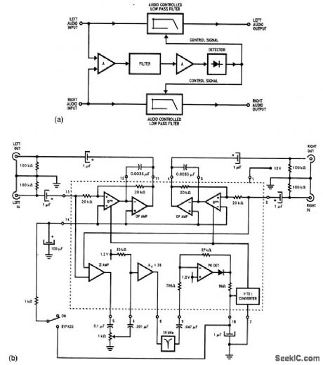
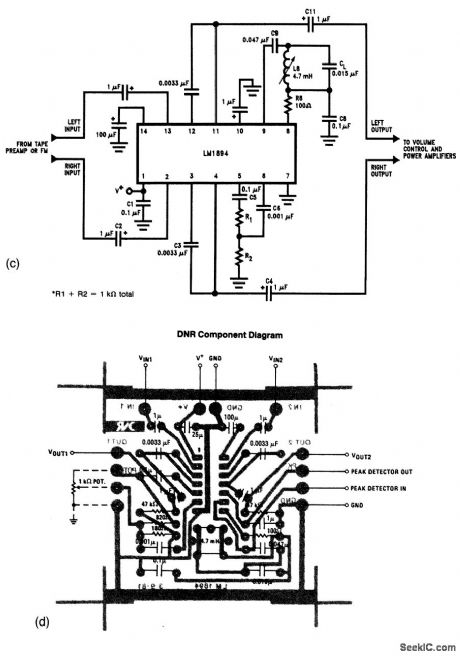
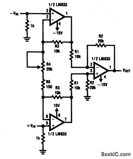
Figure 1-49A shows the block diagram, and Figs. 1-49B and 1-49C show the full schematic details of noncomplementary or dynamic noise-reduction (NR) systems. Complementary NR systems require that certain frequencies be emphasized during recording, then de-emphasized during playback in a comple-mentary mode. That is, if highs are emphasized during recording, highs are de-emphasized during playback. These noncomplementary circuits can be applied to any stereo audio system, without regard as to how the material was recorded.Both the left and right audio paths are controlled by signals derived from the mixed audio input (after filtering, amplification, and detection), all of which occurs in the LM1894. The circuits must be placed immediately after the source preamp, and before any circuit that includes user controls (volume, tone, etc.). L8 in Fig. 1-49C is part of a 19-kHz notch filter, and is adjusted to remove the FM pilot signal. R1 and R2 in Fig. 1 -49C set overall gain, as does the 1-kΩ pot in Fig. 1-49B. The 1-kΩ pot is adjusted for best noise reduction of a given program material. Figure 1-49D shows the PC layout for the circuit of Fig. 1-49B. (View)
View full Circuit Diagram | Comments | Reading(2534)
READ_HEAD_PREAMPLIFIER
Published:2009/7/6 2:24:00 Author:May
Choosing dc rather than ac coupling can reduce much of the noise associated with preamplifiers for a magnetic reading head, particularly in the low frequencies. The LM1897 eliminates the need for the capacitor that usually ac couples the read head to the preamplifier input. The read head itself has a small resistance, typically 50Ω, and so is less prone to noise pickup. Moreover, the LM1897 has a low-bias current; merely 2 μA as a worst case. Such a low-bias current flowing through the head's low resistance generates very little noise. Accordingly, even with a gain of 25, the first stage of the preamplifier circuit produces little noise. (View)
View full Circuit Diagram | Comments | Reading(1045)
0_25_V_WITH_FOLDBACK_CURRENT_LIMITING
Published:2009/7/6 2:24:00 Author:May
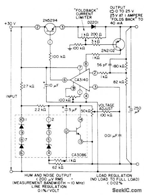
When D2201 diode senses load current of 1 A at maximum regulated output of 25V,2N2102 current-sensing transistor provides foldback of output current to 40 mA. Arrangement permits use of 2N5294 transistoras series-pass element,using only small heatsink. High-impedance reference-voltage divider across 30-V supply serves CA3140 connected as noninverting power opamp.- Linear Integrated Circuits and MOS/FET's, RCA Solid State Division, Somerville, NJ, 1977, p 248-257. (View)
View full Circuit Diagram | Comments | Reading(1551)
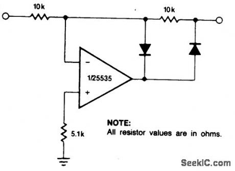
HALF_WAVE_RECTIFIER
Published:2009/7/6 2:24:00 Author:May
Circuit Notes
The circuit provides for accurate half-wave rectification of the incoming signal. For positive signals, the gain is 0; for negative signals, the gain is -1. By reversing both diodes, the polarity can be inverted. This circuit provides an accurate output, but the output impedance differs for the two input polarities and buffering may be needed. The output must slew through two diode drops when the input polarity reverses. The NE5535 device will work up to 10 kHz with less than 5% distortion. (View)
View full Circuit Diagram | Comments | Reading(0)
10_MC_SCHMITT
Published:2009/7/23 21:15:00 Author:Jessie
Will operate as square wave generator in range of 100 cps to 10 Mc, using 2N695, 2N705, or 2N711 mesa transistors.-P. A. Mclnnis, Low-Cost Computer Circuits, Motorola Application Note AN-130, Nov. 1965. (View)
View full Circuit Diagram | Comments | Reading(785)
OUT_OF_BOUNDS_PULSE_WIDTH_DETECTOR
Published:2009/7/6 2:24:00 Author:May
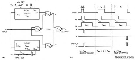
Requiring only two ICs to monitor a train of positive pulses, this circuit produces a single positive output pulse for each input pulse whose duration is either too long or too short. You specify the minimum and maximum limits by adjusting the trimming potentiometers, R1 and R2. You can set the value of the acceptable pulse width from approximately 50 ns to 10 μs, for a 74123 monostable multivibrator. The leading edge of an input pulse triggers one shots ICIA and ICIB as you can see from the timing diagram. Each NAND-gate output is high unless either or both inputs are low, so outputs X and Y are high unless the circuit encounters an out-of-range pulse. IC2D then gates a negative pulse from IC2B or IC2C to produce the circuit's positive output pulse. (View)
View full Circuit Diagram | Comments | Reading(1265)
Large_signal_voltage_follower_with_000065_worst_case_accuracy_error
Published:2009/7/23 21:15:00 Author:Jessie
The input offset voltage and drift with temperature of the RC4097 that are shown in this voltage-follower circuit are trimmed at wafer test to a low level. However, if further adjustment of VOS is necessary, nulling with the circuit of Fig. 10-17B will not degrade drift with temperature. The Fig. 10-17B offset circuit has an approximate range of about 4 mV. (View)
View full Circuit Diagram | Comments | Reading(932)
12V_AT_20A
Published:2009/7/6 2:23:00 Author:May
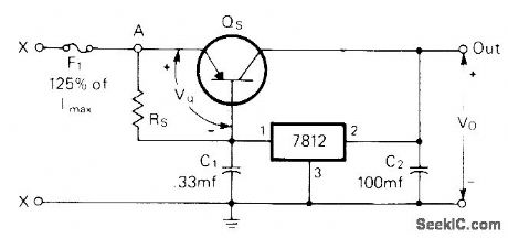
Regulator conducts and regulates until current demand is such that IR drop across RS is sufficient to overcome base-emitter junction potential of switch transistor QS, which is two 2N174 germanium transistors in parallel. Use 2 ohms for RS. QS is then turned on, with current/voltage regulation to its base controlled by regulator. Input voltage of 7812 regulatorshould be 2 V more than desired output voltage.
Article gives three different rectifier circuits suitable for use with regulator.-A. M. Clarke,Regulated 200 Watt-12 Volt D.C. Power Supply, CQ, Oct. 1975, p 28-30 and 78-79. (View)
View full Circuit Diagram | Comments | Reading(2042)
High_speed_video_peak_detector
Published:2009/7/23 21:15:00 Author:Jessie
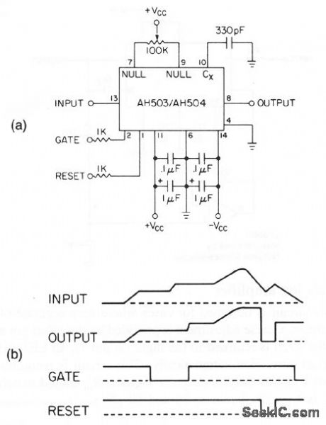
This circuit shows an AH503 or AH504 connected as a video-peak sensor or detector, using a minimum of extemal components. Figure 3-60B shows the related waveforms. The circuit will accommodate a 10-V pulse, and will capture individual 1-V pulses as narrow as 100 ns to within ± 10 mV. Delay between input peak and output settling is 500 ns. (View)
View full Circuit Diagram | Comments | Reading(670)
SIMPLIFIED_FULL_WAVE_UJT_SCR_TRIGGER
Published:2009/7/23 21:14:00 Author:Jessie
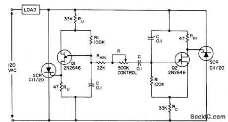
Consists of two basic half-wave circuits plated back to back, with emitters of ujt's cross-coupled with network that exerts full-cycle phase control over both scr's.- Transistor Manual, Seventh Edition, General Electric Co., 1964, p 330. (View)
View full Circuit Diagram | Comments | Reading(2000)
Low_duty_cycle_log_amplifier
Published:2009/7/23 21:13:00 Author:Jessie
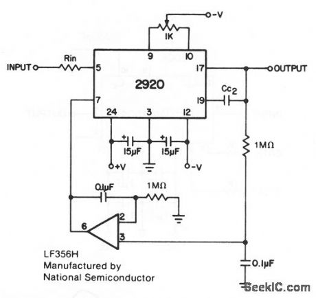
This circuit is designed for cases where very accurate offset adjustments must be made. Coarse adjustment is provided by the offset pot at pins 9/10.The output of the 2920 is returned to the input (at pin 7), an LF356H op amp to provide soft offset correction automatically. This circuit is recommended when processing bipolar or low duty-cycle pulse signals. Rin, should match the source impedance. C2 is typically between 10 and 50 pF. (View)
View full Circuit Diagram | Comments | Reading(751)
Transformerless_microphone_preamplifier_with_low_noise_inputs
Published:2009/7/23 21:13:00 Author:Jessie
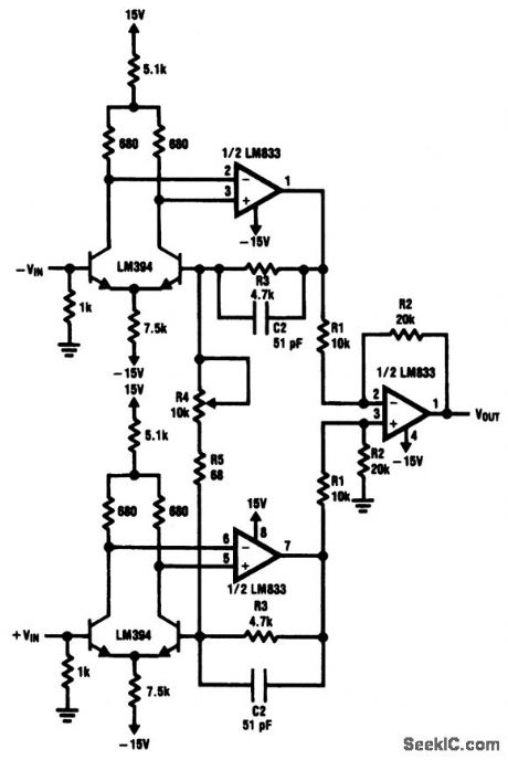
This circuit is similar to that of Fig. 1-47, except that two LM394s are used as input devices for the LM833 gain stages. The equivalent input noise of the Fig. 1-48 circuit is about 340 nV over a 20-Hz to 20-kHz band (-129 dB referred to 1V). (View)
View full Circuit Diagram | Comments | Reading(1624)
PARALLELING_REGU_LATORS
Published:2009/7/6 2:23:00 Author:May
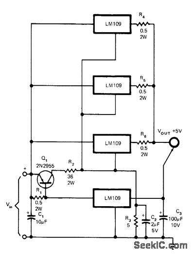
Current-sharing problem is overcome without sacrificing ripple rejection or load regulation, by using bottom regulator as control device that supplies most of load current until current through this regulator reaches about 1.3 A. At this point Q1 turns on and raises output voltage of other regulators to supply additional load current de-mands. Circuit shown will supply up to 6A for minimum input voltage of 8V. For optimum regulation, minimum load current should be 1 A.-C. T. Nelson, Power Distribution and Regulation Can Be Simple, Cheap and Rugged, EDN Magazine, Feb. 20, 1973, p 52-58. (View)
View full Circuit Diagram | Comments | Reading(628)
Precision_absolute_value_amplifier_with_low_TO_TC_VSUBOS_SUB
Published:2009/7/23 21:13:00 Author:Jessie
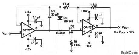
The high gain and low temperature-coefficient output offset voltage of the OP-77E assures accurate operation with inputs from microvolts to volts. In this circuit, the signal always appears as a common-mode signal to the op amps. The OP-77E CMRR of 1 μV/V assures errors of loss than 2 ppm. (View)
View full Circuit Diagram | Comments | Reading(994)
AUTOMOBILE_LOCATER
Published:2009/7/6 2:22:00 Author:May
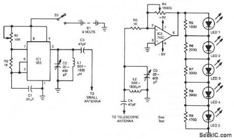
This locater is made up of two parts. The first is an rf oscillator, whose circuit is shown in Fig. 8-4a.The second is a sensitive receiver shown in Fig. 8-4b. The heart of the oscillator is a 555 timer IC. Tank circuit C2 and L1 is used to tune the transmitter. The antenna is coupled to the transmitter through C3. A telescopic antenna or a length of hookup wire will work quite well. At the receiver, the incoming signal is tuned by C5 and L2 before being passed on to the 741 IC. The five LEDs are used to indicate signal strength, they light up in order (1 to 5) as the signal gets stronger.
After the devices are built, the receiver and transmitter will need to be tuned. Tune the transmitter until all of the receiver's LEDs light. Separate the receiver and the transmitter-the farther apart they are the better-and adjust R4 until you get a maximum strength reading only when the receiver's antenna is pointed directly at the transmitter. Place the transmitter on the dashboard and completely extend the antenna. To find your car, just extend the telescope antenna to its full length and hold it parallel to the ground. Point the antenna to your far left, then swing it to your far right. Do that until you find in which direction the strongest signal lies, as indicated by the LEDs. The antenna will be pointing at your car. (View)
View full Circuit Diagram | Comments | Reading(888)
12_V_SHUNT_AT_5_mA
Published:2009/7/6 2:22:00 Author:May

Low-power shunt regulator uses opamp to absorb excess load current. Value of R1 is chosen to step up reference voltage of 5.6-V zener to +12V at 5 mA. Design procedure for other output voltages is given. Output impedance is 0.01 ohm at 100 Hz, giving 120-Hz ripple-frequency filtering comparable to that of 100,000-μF capacitor-W.G. Jung, IC Op-Amp Cookbook, Howard W.Sams, Indianapolis, IN, 1974, p 166-168. (View)
View full Circuit Diagram | Comments | Reading(912)
Transformerless_microphone_preamplifier
Published:2009/7/23 21:12:00 Author:Jessie
This circuit uses two LM833s to amplify the input signal before the common-mode noise is cancelled in the differential amplifier. The equivalent input noise is about 760 nV over a 20-Hz to 20-kHz frequency band (-122 dB referred to 1V), which is over 26 dB lower than a typical microphone output from the 30-dB SPL ambient noise level in a quiet room. THD is under 0.01% at maximum gain, and 0.002% at minimum gain. R4 adjusts the circuit gain from about 4 to 270.Common-mode noise is about 60 dB (or 44 dB, worst case) when R1, R2, and R3 are of 0.1 % tolerance. If better common-mode rejection is needed, one or the R2s can be replaced with an 18-kΩ resistor and a 5-kΩ, pot to trim for a better CMRR.If necessary, use 470-pF capacitors between inputs and ground to prevent RF interference from entering the preamp inputs. (View)
View full Circuit Diagram | Comments | Reading(1115)
ABSOLUTE_VALUE_IDEAL_FULL_WAVE_RECTIFIER
Published:2009/7/6 2:22:00 Author:May
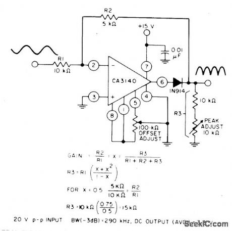
Circuit Notes
The circuit uses a CA3140 BiMOS op amp in an inverting gain configuration. When equality of two equations shown in satisfied, full-wave output of ctrcuit is symmetril. (View)
View full Circuit Diagram | Comments | Reading(881)
5_V_FROM_48_V
Published:2009/7/6 2:21:00 Author:May
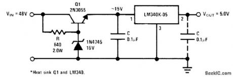
Combillation of zener and resistor R gives equivalent of power zener as solution to regulator protection problem when input voltage is much higher than rated maximum of regulator. Maximum load is 1A. With optional capacitor,circuit noise is only 700μV P-P.-″Linear Applications、Vol.2、″ National Semiconductor,Santa Clara,CA、1976、AN-103,p 10. (View)
View full Circuit Diagram | Comments | Reading(763)
255_FREQUENCY_SYNTHESIZER
Published:2009/7/6 2:21:00 Author:May
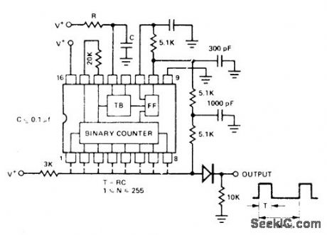
Circuit as shown for programmable counter section of Exar XR-2240 programmable timer/counter provides square-wave outputs at 255 discrete frequencies from given internal time-base setting.Output is positive pulse train with pulse width T determined by values of R and C. Period is equal to (N + 1)T where N is programmed count in counter of IC. Counter output connections to output bus determine value of N; if pins 1,3,and 4 are connected to bus, N is 1 + 4 + 8 or 13 and period is 14T, Supply voltage range is 4-.15 V.If counter cannot be triggered when using supplyabove 7V and less than 0.1μF forC, connect 300 pF from pin 14 to ground.- Timer Data Book, Exar Integrated Systems, Sunnyvale, CA, 1978, p 11-18. (View)
View full Circuit Diagram | Comments | Reading(890)
| Pages:1056/2234 At 2010411042104310441045104610471048104910501051105210531054105510561057105810591060Under 20 |
Circuit Categories
power supply circuit
Amplifier Circuit
Basic Circuit
LED and Light Circuit
Sensor Circuit
Signal Processing
Electrical Equipment Circuit
Control Circuit
Remote Control Circuit
A/D-D/A Converter Circuit
Audio Circuit
Measuring and Test Circuit
Communication Circuit
Computer-Related Circuit
555 Circuit
Automotive Circuit
Repairing Circuit