
Circuit Diagram
Index 1045
2_METER_POWER_AMPLIFIER
Published:2009/7/6 5:09:00 Author:May

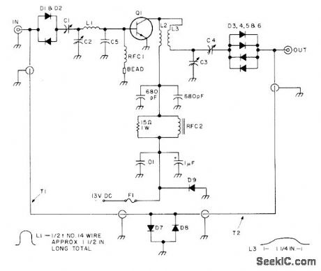
Provides 10-dB gain with full 30-W output at 160MHz and about 0.5-dB more gain at 150 MHz, using Motorola MRF238 transistor. C1-C4 are Arco 463, 464 or 424. RFC1 is 10 turns No. 20 on 270-ohm 1/2-W resistor. C5 is three 90-pF silver mica in parallel.RFC2 is 6 to 8 turns No. 18on toroid. L1 is 1/2turn No. 141 1/2inch long. L2 is 4 turns No. 14 spaced on 1/4inch diameter. L3 is 1 1/4-inch curve of No.14. D1-D8 are 1N4148. T1 and T2 are one quarter-wavelength of RG-174 or similar 50-ohm coax. D9 is 2-A silicon rectifier.-D. J.Lynch, Build a 2m Power Amp, 73 Magazine, Nov. 1977, p 96-97. (View)
View full Circuit Diagram | Comments | Reading(2547)
SENSITIVE_FIELD_STRENGTH_METER
Published:2009/7/6 5:09:00 Author:May
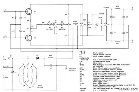
The two-pole, five-position switch, coils and 365-pF variable capacitor cover a range from 1.5 to 30 MHz. The amplifier uses Darlington npn transistors whose high beta, 5000, provides high sensitivity with S1 used as the amplifier on/off switch. Switch S2 in the left position allows the output of the 1N34 diode to be fed directly into the 50-μA meter (M) for direct reading. When S2 is in the right position, the amplifier is switched into the circuit. Switch S3 is for local or remote monitoring. At full gain setting, the input signal is adjusted to give a full-scale reading of 50 mA on the meter. Then with the amplifier switched out of the circuit, the meter reading drops down to about 0.5 mA. A 2.5-mH rf choke and capacitors C3, C4, and C5 effectively keep rf out of the amplifier circuit. (View)
View full Circuit Diagram | Comments | Reading(2353)
LOW_BATTERY_WARNING
Published:2009/7/6 5:07:00 Author:May
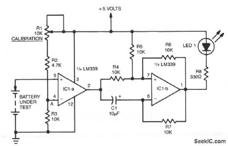
A voltage divider consisting of R1, R2, and R3 is used to set the input reference voltage below which the batteries are to be replaced. That reference voltage, at point A, is varied by R1. With the voltage divider shown in Fig. 9-7, a range of 2 to 3.5 V is possible. When the battery voltage drops below that at point A, the output of IC1a, 1/4 of a LM339 quad comparator, switches from high to low. That triggers IC1b, which is configured as an astable multivibrator. Feedback resistors R6 and R7, coupled with capacitor C1,determine the time constant of the multiibrator. The output from IC1b is connected to LED1 through dropping resistor R8. With the circuit values as shown, the LED will flash at a rate of 3 Hz.Although this circuit was designed specifically to monitor RAM back-up batteries, it can of course be modified for use in just about any application where the condition of a battery must be found. (View)
View full Circuit Diagram | Comments | Reading(1396)
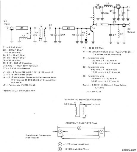
A_10_WATT_225_400_MHz_AMPLIFIER
Published:2009/7/6 5:06:00 Author:May
Circuit Notes
This broadband amplifier covers the 225-400 MHz military communications band producing 10 watt RF output power and operating from a 28 volt supply. The amplifier can be used as a driver for higher power devices such as 2N6439 and MRF327. The circuit is designed to be driven by a 50 ohm source and operate into a nominal 50 ohm load. The input matching network consists of a section composed of C3, C4, Z2, C5 and C6. C2 is a dc blocking capacitor, and T1 is a 4:1 impedance ratio coaxial transformer.Z1 is a 50 ohm transmission line. A compensation network consisting of R1, C1, and L1 is used to improve the input VSWR and flatten the gain response of the amplifier.L2 and a small ferrite bead make up the base bias choke. The output network is made up of a microstrip L-section consisting of Z3 and C7, and a high pass section consisting of C8 and L3. C8 also serves as a dc blocking capacitor. Collector decoupling is accom-plished through the use of L4, L5, C9, C10, C11, C12, and C13. (View)
View full Circuit Diagram | Comments | Reading(1518)
TONE_BURST_GENERATOR
Published:2009/7/6 5:05:00 Author:May
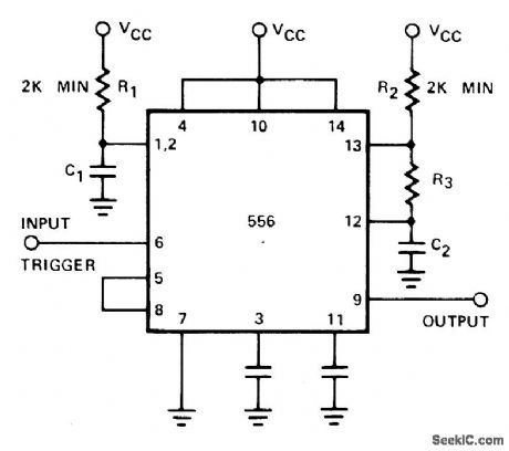
The dual timer makes an excellent tone burst generator. The first half is connected as a one shot and the second half as an oscillator.
The pulse established by the one shot turns on the oscillator allowing a burst of pulses to be generated. (View)
View full Circuit Diagram | Comments | Reading(0)
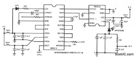
50_Mb_s_FIBER_OPTIC_RECEIVER
Published:2009/7/6 5:04:00 Author:May
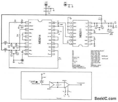
The optical signal is coupled to the pin diode. Current flowing in the diode also flows into the input of the NE5211 preamplifier. The preamplifter is a fixed-gain block that has a 28-KΩ differential transimpedance and does a single-ended to differential conversion. With the signal in differential form, greater noise immunity is assured. The second stage, or postamplifter NE5214, includes a gain block, auto-zero detection, and limiting. The auto-zero circuit allows dc coupling of the preamplifier and the postamplifter and cancels the signal dependent offset because of the optical-to-electrical conversion. The auto-zero capacitor must be 1000 pF or greater for proper operation. The peak detector has an external threshold adjust-ment, RTH, allowing the system designer to tailor the threshold to the individual's need. Hysteresis included to minimize jitter introduced by the peak detector, and an extemal resistor, RHYS, is used to set the amount of hysteresis desired. The output stage provides a single-ended TTL data signal with matched rise and fall times to minimize duty-cycle distortion. (View)
View full Circuit Diagram | Comments | Reading(1248)
IMPROVED_RF_ISOLATION_AMPLIFIER
Published:2009/7/6 5:03:00 Author:May
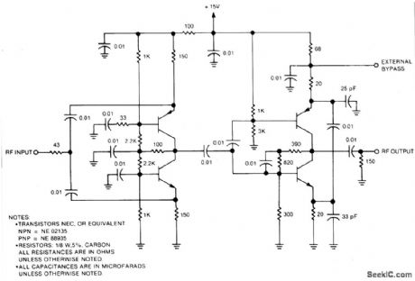
Circuit Notes
This wideband RF isolation amplifier has a frequency response of 0.5 to 400MHz±0.5dB. This two stage amplifier can be used in applications requiring high reverse isolation, such as receiver intermediate-frequency (IF) strips and frequency distribution systems. Both stages use complementary-symmetry transistor arrangements. The input stage is a common-base connection for the complementary circuit. The output stage, which supplies the positive gain, is a common-emitter circuit using emitter degeneration and collector-base feedback for impedance control. (View)
View full Circuit Diagram | Comments | Reading(1998)
STROBE_TONE_BURST_GENERATOR
Published:2009/7/6 5:02:00 Author:May
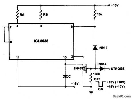
View full Circuit Diagram | Comments | Reading(1499)
SINGLE_TIMER_IC_PROVIDES_SQUARE_WAVE_TONE_BURSTS
Published:2009/7/6 5:01:00 Author:May
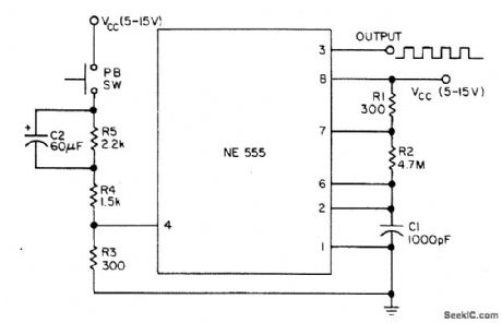
The tone-burst generator gives a 50-ms burst of 1.5 kHz square waves with each operation of the pushbutton and can source or sink 200 mA. (View)
View full Circuit Diagram | Comments | Reading(644)
05_25_kHz_TRIANGLE
Published:2009/7/6 5:01:00 Author:May
Diode bridge and FET form constant-current source charging c1,to make voltage across c1 change at linear rate as required for triangle output across c1. Frequenεy can be adjusted from 500 Hz to above 20 kHz with constant output amρlitude, by means of R1 Short -term stabilityis better than1 partin l0.000 Since the same R and C are used to generate both sections of the waveform,ρositive and negative slopes are identical,Diodesare HP 5082-2810.-G. R. Begaulg, oρ AmρMakes Variable-Frequency Tliangular Wave Generator,EDN Magazine, Sept 15,1972,ρ 42-43.
(View)
View full Circuit Diagram | Comments | Reading(858)
BROADCAST_BAND_PF_AMPLIFIER
Published:2009/7/6 4:59:00 Author:May
Circuit Notes
The circuit has a frequency response ranging from 100 Hz to 3 MHz; gain is about 30 dB. Field-effect transistor Q1 is configured in the common-source self-biased mode; optional resistor R1 sets the input impedance to any desired value. Commonly, it will be 50 ohms. The signal is then direct-coupled to Q2, a common-base circuit that isolates the input and output stages and provides the amplifier's exceptional stability. Q3 functions as an emitter follower, to provide low output impedance (about 50 ohms). For higher output impedance, include resistor R8. It will affect impedance according to this formula: R8~Rout-50. Otherwise, connect output capacitor C4 directly to the emitter of Q3. (View)
View full Circuit Diagram | Comments | Reading(929)
UNIVERSAL_BATTERY_CHARGER_1
Published:2009/7/6 4:59:00 Author:May

The charger's output voltage is adjustable and regulated, and has an adjustable constant-current charging circuit that makes it easy to use with most NiCad batteries. The charger can charge a single cell or a number of series-connected cells up to a maximum of 18 V.
Power transistors Q1 and Q2 are connected as series regulators to control the battery charger's output voltage and charge-current rate. An LM317 adjustable voltage regulator supplies the drive signal to the bases of power transistors Q1 and Q2. Potentiometer R9 sets the output-voltage level. A current-sampling resistor, R8 (a 0.1- Ω, 5-W unit), is connected between the negative output lead and circuit ground. For each amp of charging that flows through R8, a 100 mV output is developed across it. The voltage developed across R8 is fed to one input of comparator U3. The other input of the comparator is connected to variable resistor R10.
As the charging voltage across the battery begins to drop, the current through R8 decreases. Then the voltage feeding pin 5 of U3 decreases, and the comparator output follows, turning Q3 back off, which completes the signal's circular path to regulate the battery's charging current.
The charging current can be set by adjusting R10 for the desired current. The circuit's output voltage is set by R9. (View)
View full Circuit Diagram | Comments | Reading(2040)
SQUARE_WAVEFORM_MULTIBURST_GENERATOR
Published:2009/7/6 4:55:00 Author:May
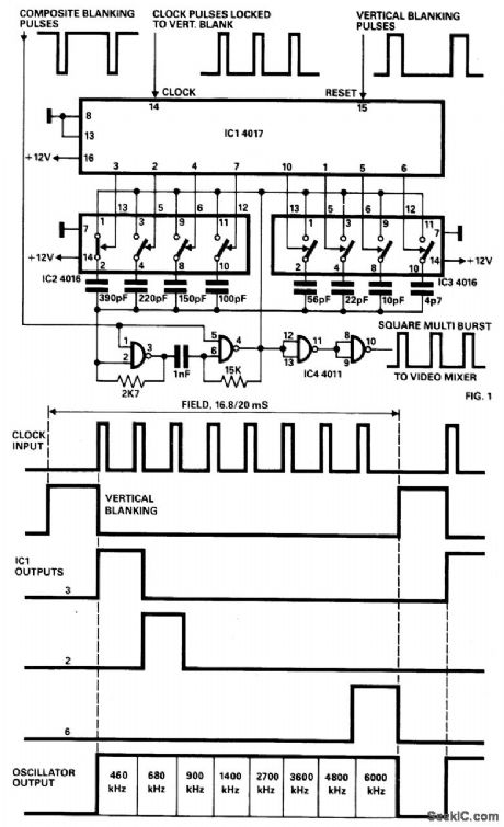
The generator described here IS intended for multiburst signal square waveformgeneration and can be used as a device for characterizing the response of TV monitoramplifiers as shown.The circuit is an RC oscillator with NAND gates(IC4-4011),withits capacitor C changed periodically by means of bilateral switches(IC2,IC3-4016),Thecontrol inputs of bilateral switches are driven by the outputs of a counter/decoder(IC1-4017)the operation of which is determined by generated clock pulses,SO that theyoccur eight times at half-picture (field).These pulses are locked to vertical blank pulses. Horizontal synchronizatiOn is achieved by means of composite blanking pulses (negative polarization) applied to pms 1 and 5 of IC4,The oscillator frequency changesh the following(liscrete steps:460 kHz,680 kHz,900 kHz,1400 kHz,2700 kHz,3600kHz,for the time of one frame。The video signal is fed on a mlxer where it is superimposedwith a composite sync signal. (View)
View full Circuit Diagram | Comments | Reading(1128)
DIGITAL_FIBER_OPTIC_RECEIVER
Published:2009/7/6 4:54:00 Author:May
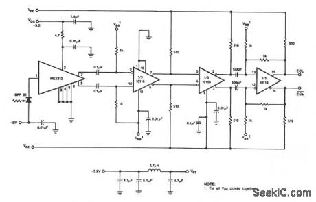
This receiver uses the NE5212, the Signetics 10116 ECL line receiver, and the Phillips/Amperex BPF31 pin diode. The circuit is a capacitor-coupled receiver and utilizes positive feedback in the last stage to provide the hysteresis. The amount of hysteresis can be tailored to the individual application by changing the values of the feedback resistors to maintain the desired balance between noise immunity and sensitivity. At room temperature, the circuit operates at 50-M baud with a BER of 10E-10 and over the automotive temperature range at 40-M baud with a BER of 10E-9. Higher speed experimental diodes have been used to operate this circuit at 220-M baud with a BER of 10E-10. (View)
View full Circuit Diagram | Comments | Reading(1536)
6_METER_KILOWATT_AMPLIFIER
Published:2009/7/6 4:54:00 Author:May
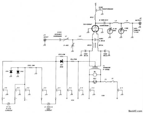
Circuit Notes
The amplifier uses a grounded grid circuit with either the Eimac 3CX1000A7 or 8877, ceramic/metal triodes intended for linear service in the HP and VHF ranges. The amp provides the legal power output of 1500 watts PEP and CW service with no effort and requires a driver delivering between 50 and 80 watts at 50 MHz. With a plate voltage of 3000 volts at 0.8 amps the amplifier performs at 60 percent efficiency. The grid is grounded by means of the grid ring of the 3CX1000A7 socket providing a lowinductance path to ground. The amplifier is completely stable. (View)
View full Circuit Diagram | Comments | Reading(3577)
SINGLE_TONE_BURST_GENERATOR
Published:2009/7/6 4:53:00 Author:May
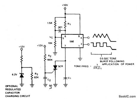
The tone burst generator supplies a tone for one-half second after the power supply is activated; its intended use is a communications network alert signal. Cessation of the tone is accomplished at the SCR, which shunts the timing capacitor C1 charge current when activated. The SCR is gated on when C2 charges up to the gate voltage which occurs in 0.5 seconds. Since only 70 μA are available for triggering, the SCR must be sensitive enough to trigger at this level. The triggering current can be increased, of course, by reducing R2 (and increasing C2 to keep the same time constant). If the tone duration must be constant under widely varying supply voltage conditions, the optional Zener diode regulator circuit can be added, along with the new value for R2 R2' = 82 kΩ. If the SCR is replaced by an can transistor, the tone can be switched on and off at will at the transistor base terminal. (View)
View full Circuit Diagram | Comments | Reading(982)
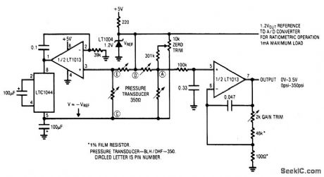
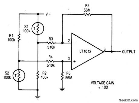
STRAIN_GAUGE_BRIDGE_SIGNAL_CONDITIONER
Published:2009/7/6 4:50:00 Author:May
View full Circuit Diagram | Comments | Reading(683)
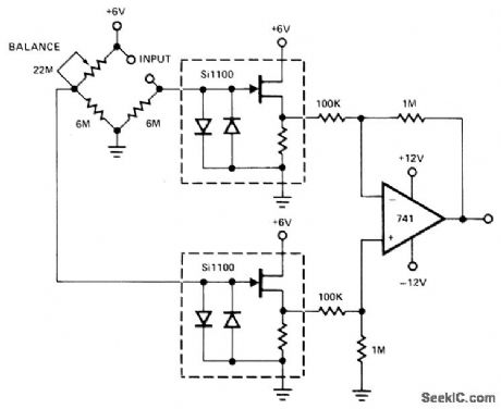
AMPLIFIER_FOR_BRIDGE_TRANSDUCERS
Published:2009/7/6 4:47:00 Author:May
View full Circuit Diagram | Comments | Reading(912)
LOW_POWER_COMMON_SOURCE_AMPLIFIER
Published:2009/7/6 4:47:00 Author:May
A circuit that will operate in the 10- to 20- microamp range at a 12-volt supply voltage. The diode protection is available in this configuration. The circuit voltage gain will be between 10 and 20, with extremely low power consumption (approximately 250 μW).This is very desirable for remote or battery operation where minimum maintenance is important. (View)
View full Circuit Diagram | Comments | Reading(855)
LOW_COST_100_M_BAUD_FIBER_OPTIC_RECEIVER
Published:2009/7/6 4:46:00 Author:May
This two-chip receiver with minimum external component count has been designed for low-cost fiber optic applications to 100-M baud (50 MHz). The receiver is divided into pre- and postamplifier ICs for increased stability. The preamplifier IC features low noise with a differential transresistance design. The postamplifier IC incorporates an auto-zeroed first stage with noise shaping, high-gain symmetrical-limiting amplifier, and a matched rise/fall time TTL output buffer. A wide-band full-wave rectifier functions as a link-status indicator. To ensure stability, a surface mount, small outline (SO), package is used. The received signal in the - 35 dBm optical (average) to -9 dBm range is converted into a small unipolar current by the pin diode. The pin diode then feeds its signal current to a preamplifier, such as the NE5212.The preamplifier output is fed to a high-gain limiting amplifier, simply known as the post amp.
The NE5214/NE5217 postamplifters are low-cost ICs that provide up to 60 dB of gain at 50 MHz to bring mV level signals up to TTL levels. The postamplifter IC incorporates an auto-zeroed first stage with noise shaping, a high-gain symmetrical-limiting amplifier, and a matched rise/fall time TTL output buffer. A secondary amplifier chain functions as a link-status indicator. (View)
View full Circuit Diagram | Comments | Reading(1132)
| Pages:1045/2234 At 2010411042104310441045104610471048104910501051105210531054105510561057105810591060Under 20 |
Circuit Categories
power supply circuit
Amplifier Circuit
Basic Circuit
LED and Light Circuit
Sensor Circuit
Signal Processing
Electrical Equipment Circuit
Control Circuit
Remote Control Circuit
A/D-D/A Converter Circuit
Audio Circuit
Measuring and Test Circuit
Communication Circuit
Computer-Related Circuit
555 Circuit
Automotive Circuit
Repairing Circuit