
Circuit Diagram
Index 1042
COMMON_MODE_VOLUME_AND_TONE_CONTROL
Published:2009/7/6 5:48:00 Author:May
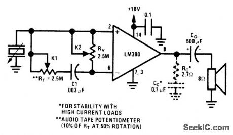
Eliminates attenuation of signal by conventional voltage-divider type of volume control and gives maximum input impedance. Used with transducers having high source impedance, but will also serve with low-impedance transducers.- Audio Handbook, National Semiconductor, Santa Clara, CA, 1977, p 4-21-4-28. (View)
View full Circuit Diagram | Comments | Reading(777)
“HEE_HAW_TWO_TONE_SIREN
Published:2009/7/6 5:47:00 Author:May
The circuit uses two gates of a 7400 IC cross-connected to form an astable multivibrator driven by the 1-pulse per second output of the digital clock IC. The hee-haw circuit has a low frequency astable modulator added to make a selfcontained European-type siren. Tone and rate can be varied as desired by changing capacitor values. If the tone is too harsh, a simple R-C ftlter will remove the harmonic content-the multivibrator output is almost a square wave. With the resistor values shown, no start-up problems occur; but if the 2.2 k or 2.7 k resistors are changed too much, latch-up can be a problem. (View)
View full Circuit Diagram | Comments | Reading(2988)
12_V_PHONO_PREAMP
Published:2009/7/6 5:47:00 Author:May
Low-noise circuit has midband 0-dB reference gain of 46 dB. Designed for RIAA response. Internal resistor matrix of IC minimizes parts count. Input is from magnetic cartridge.- Audio Handbook, National Semi-conductor, Santa Clara, CA, 1977, p 2-25-2-31. (View)
View full Circuit Diagram | Comments | Reading(781)
RUMBLE_FILTER
Published:2009/7/6 5:46:00 Author:May
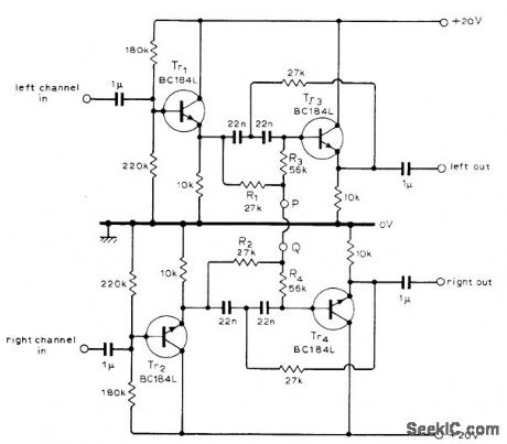
Used when rumble from cheaper turntable or record extends above 100 Hz, causing disconcerting out-of-phase loud-speaker signals, Circuit is based on fact that human ear is not sensitive to directional information below about 400 Hz, making it permissible to remove stereo (L – R) signal at low frequencies and thus remove stereo rumble without losing stereo separation. Emitter-followers feed high-pass filters having 200-Hz breakpoint frequencies and Butterworth characteristics. Attenuation of filter is 12 dB at 100 Hz. Filter circuit can be disabled by placing switch between points P and Q.-M. L. Oldfield, Stereo Rumble Filter, Wireless World, Oct. 1975, p 474. (View)
View full Circuit Diagram | Comments | Reading(5992)
HIGH_POWER_SIREN
Published:2009/7/6 5:46:00 Author:May
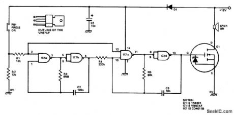
IC1a and IC1b are wired as a slow astable multivibrator and IC1c-IC1d are wired as a fast astable. Both are gated types, which can be turned on and off via PB1. The output of the slow astable modulates the frequency of the fast astable, and the output of the fast astable is fed to the external speaker via the Q1 VMOS power FET amplifier stage. (View)
View full Circuit Diagram | Comments | Reading(872)
YELP_OSCILLATOR
Published:2009/7/6 5:44:00 Author:May

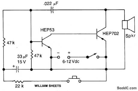
Close the pushbutton switch and the circuit starts the siren up-shifting to a higher frequency. Release it and the tone slides down until S2 is closed again. Tone quality is adjusted by changing the 0.022 μF capacitor.
(View)
View full Circuit Diagram | Comments | Reading(863)
SIREN_ALARM_SIMULATES_STAR_TREK_RED_ALERT
Published:2009/7/6 5:43:00 Author:May
The signal starts at a low frequency, rises for about 1.15 seconds to a high frequency, ceases for about 0.35 seconds, then starts rising again from a low frequency, and so on ad infinitum. (View)
View full Circuit Diagram | Comments | Reading(1725)
Three_op_amp_instrumentation_amplifier
Published:2009/7/23 21:11:00 Author:Jessie
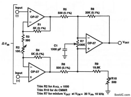
This circuit uses only OP-37 ICs for instrumentation applications, whore low noise, wide bandwidth, low input-offset TC, and low input-bias currents are required.
(View)
View full Circuit Diagram | Comments | Reading(878)
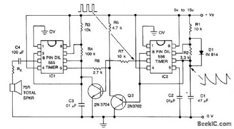
60_Hz_CLOCK_PULSE_GENERATOR
Published:2009/7/6 5:42:00 Author:May
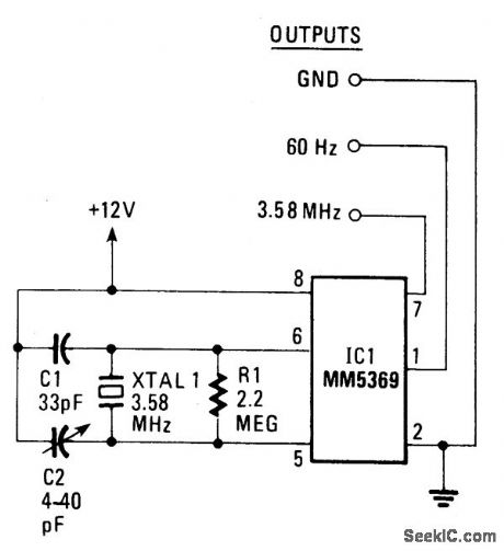
The circuit provides a clean, stable square wave and it will operate on anywhere from 6 to 15 volts. The IC and color-burst crystal are the kind used in TV receivers. The 3.58 MHz output makes a handy marker signal for shortwave bands. (View)
View full Circuit Diagram | Comments | Reading(999)
Coaxial_line_driver
Published:2009/7/23 21:10:00 Author:Jessie
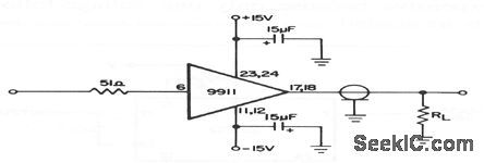
This circuit shows a 9911 used to drive long coaxial lines in a 50- or 75-Ω system, such as those found in test equipment and other applications. The 9911 is a high-current voltage follower and, in this application, is capable of driving long cables (and thus large capacitances) without instabilities. Remember that the 9911 provides 0.96 gain, which can drop to 0.90 when the chip is heavily loaded. RL should match the cable impedance (typically 50 or 75Ω). (View)
View full Circuit Diagram | Comments | Reading(723)
ELECTRONIC_SHIP_SIREN
Published:2009/7/6 5:40:00 Author:May
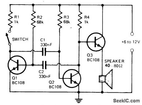
The circuit consists of a multivibrator (Q1 & Q2), and a low power output stage Q3. The speaker should have an impedance in the region of 40 to 80 ohms. To use a low impedance speaker, connect an output transformer from the emitter of Q3 to ground. C1 and C2 determine the pitch of the siren and the values specified will provide a tone of about 300 Hz.Quiescent current is negligible. The output at the collector of Q2 can also be fed into an amplifier input via a 1 pF electrolytic, in series with a 12 k resistor.
(View)
View full Circuit Diagram | Comments | Reading(947)
SIREN_USES_TTL_GATES
Published:2009/7/6 5:40:00 Author:May
The siren consists of two oscillators which generate the tones. A third oscillator is used to switch the others on and off alternately, giving the two-tone effect. By changing the capacitor values different tones can be produced. (View)
View full Circuit Diagram | Comments | Reading(574)
LOW_BATTERY_DETECTOR
Published:2009/7/6 5:39:00 Author:May
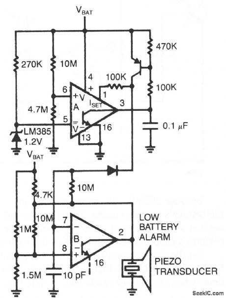
Comparator A detects when the supply voltage drops to 4 V and enables comparator B to drive a piezoelectric alarm. (View)
View full Circuit Diagram | Comments | Reading(2514)
TOY_SIREN
Published:2009/7/6 5:38:00 Author:May
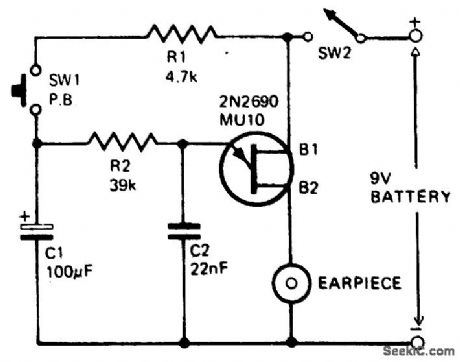
This circuit can be built small enough to fit inside a toy. The circuit consists of a relaxation oscillator utilizing one unijunction transistor (2N2646, MU10, 71543). R2 and C2 determine the frequency of the tone. Pushing the button, SW1 charges up the capacitor and the potential at the junction of R2 and C2 rises, causing an upswing in the frequency of oscillation. On releasing the pushbutton the charge on C2 will drop slowly with a proportional reduction in the frequency of oscillation. Manual operation of the button at intervals of approximately 2 seconds will produce a siren sound. (View)
View full Circuit Diagram | Comments | Reading(2525)
AUTO_BATTERY_ALTERNATOR_MONITOR
Published:2009/7/6 5:38:00 Author:May
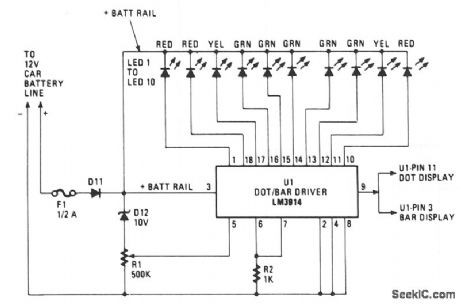
Most of the circuitry is contained in the LM3914 dot/bar-graph driver IC chip. In addition to the comparator circuitry within the package, it also contains a stable reference supply and the driv-ers for the LEDs. Resistor R2 acts as the current limiter for all the LEDs. Resistor R2 may be varied for LED brightness.
The unit will illuminate one LED for each volt-age condition encountered in the charging system.This system is called a dot-graph display; it is achieved by wiring the mode control at pin 9 to pin 11 on U1.
It is possible to wire the monitor so that each lamp will be illuminated up to the maximum voltage on the line at that moment. The latter is referred to as a bar-graph display. By connecting pin 9 to pin 3 on U1, the bar-graph mode will be enabled. (View)
View full Circuit Diagram | Comments | Reading(2471)
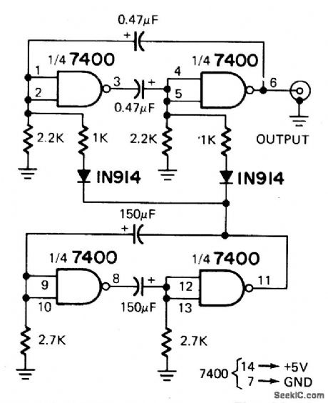
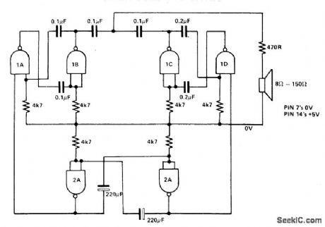
7400_SIREN
Published:2009/7/6 5:37:00 Author:May
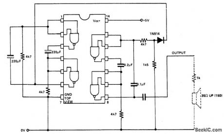
Two NAND gates are used for the oscillator, and two as the control. If the two-tone speed needs to be altered, the 220 μF capacitors can be changed (larger for slower operation). If the frequency of the oscillator is to be changed, the 0.2 and 0.1 μF capacitors can be varied and the value of R1 can be increased. To change frequency range between the two notes, alter the 1.5 k (1.500) resistor. (View)
View full Circuit Diagram | Comments | Reading(986)
Line_operated_IC_audio_amplifier
Published:2009/7/23 21:10:00 Author:Jessie
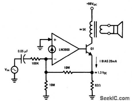
This amplifier operates from a +98-V supply (the rectified line voltage). Such amplifiers are often found in consumer products. Virtually any high-voltage transistor (capable of about 100 V from collector to emitter) can be used for Q1, which is biased and controlled by the LM3900 Norton amplifier (chapter 11). The magnitude of the dc biasing voltage, which appears across the emitter resistor of Q1 is controlled by the resistor between the (-) input of the LM3900 and ground. (View)
View full Circuit Diagram | Comments | Reading(840)
GLITCH_FREE_TURBO_CIRCUIT
Published:2009/7/6 5:36:00 Author:May
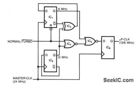
This simple circuit generates a dual-speed clock for personal computers. The circuit synchronizes your asynchronous switch inputs with the master clock to provide glitch-free transitions from one clock speed to the other. The dual-speed clock allows some programs to run at the higher clock speed in order to execute more quickly. Other programs-for example, programs that use loops for timing-can still run at the lower speed as necessary. The circuit will work with any master-clock. frequency that meets the flip-flops' minimumpulse-width specs.
The two D two flip-flops, IC1 and IC2, and an XOR gate, IC3, form a binary divider that develops the 6- and 12-MHz clocks. When the NT signal is low, the reset pin forces the 6-MHz output low. On the other hand, when the NT signal is high, IC3 blocks the 12-MHz output. Therefore, only one of the two clock signals passes through IC3 and gets clocked into IC6. Because the master-clk signal clocks IC6, asynchronous switching of the NT signal can't generate an output pulse shorter than 41 μs (1/24 MHz). Also, the synchronization eliminates glitches. (View)
View full Circuit Diagram | Comments | Reading(657)
HIGH_PERFORMANCE_SAMPLE_AND_HOLD
Published:2009/7/6 5:36:00 Author:May
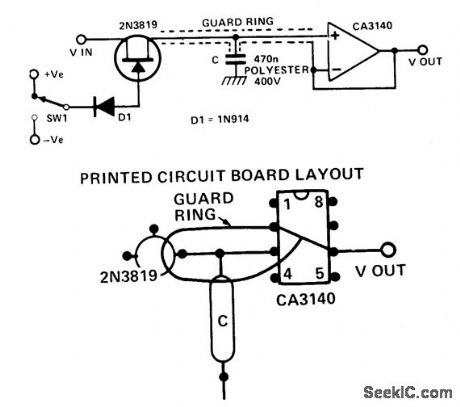
Circuit Notes
When switch SW1 is positive, the FET is turned on, and has a resistance of about 400 ohm. The input voltage charges up the capacitor through the FET. When SW1 is negative, the FET is turned off (pinched off). To get a long storage time, the op amp mus, have a very low input bias current. For the CA3140, this current is about 10 pico amps. The rate at which the capacitor will be discharged by this current is based on the equation, C (dv/dt)=i where dv/dt is the rate of change of voltage on the capacitor.Therefore: (View)
View full Circuit Diagram | Comments | Reading(676)
Wideband_amplifier_for_test_equipment_applications_high_gain
Published:2009/7/23 21:10:00 Author:Jessie
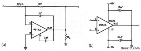
This circuit shows a 9914A used in an application where high speed at a relatively high gain is required (a gain of 100in this case). With the values given, this circuit can operate comfortably at frequencies of 20 MHz. If a lower gain is needed, connect a 1- to 5-pF capacitor between the output and inverting input to aid in suppressing parasitic oscillations. Figure 3-55B shows external connections for the 9914A. (View)
View full Circuit Diagram | Comments | Reading(743)
| Pages:1042/2234 At 2010411042104310441045104610471048104910501051105210531054105510561057105810591060Under 20 |
Circuit Categories
power supply circuit
Amplifier Circuit
Basic Circuit
LED and Light Circuit
Sensor Circuit
Signal Processing
Electrical Equipment Circuit
Control Circuit
Remote Control Circuit
A/D-D/A Converter Circuit
Audio Circuit
Measuring and Test Circuit
Communication Circuit
Computer-Related Circuit
555 Circuit
Automotive Circuit
Repairing Circuit