
Circuit Diagram
Index 1044
Voltage photoelectric sensor broken circuit and open phase protection circuit diagram
Published:2011/8/2 2:36:00 Author:Rebekka | Keyword: Voltage photoelectric sensor, broken circuit, open phase protection
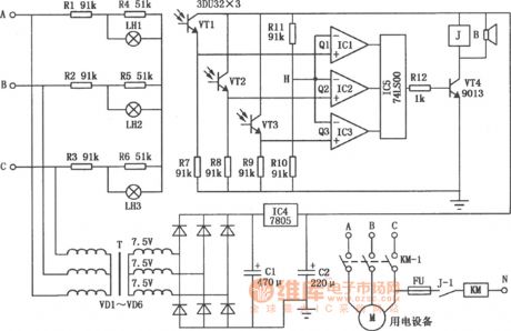
The circuit is voltage photoelectric sensor type three-phase broken circuit protector. It will make alarm sound and cut off the power supply automatically. The circuit is shown as above. (View)
View full Circuit Diagram | Comments | Reading(3264)
WAILING_ALARM
Published:2009/7/6 5:28:00 Author:May

This circuit simulates the sound of an American police siren. IC2 is wired as a low frequency astable that has a cycling period of about 6 seconds. The slowly varying ramp waveform on C1 is fed to pnp emitter follower Q1, and is then used to frequency modulate alarm generator IC1 via R6. IC1 has a natural center frequency of about 800Hz. Circuit action is such that the alarm output signal starts at a low frequengy, rises for 3 seconds to a high frequency, then falls over 3 seconds to a low frequency again, and so on ad infinitum.
(View)
View full Circuit Diagram | Comments | Reading(1557)
12_ns_CIRCUIT_BREAKER
Published:2009/7/6 5:28:00 Author:May
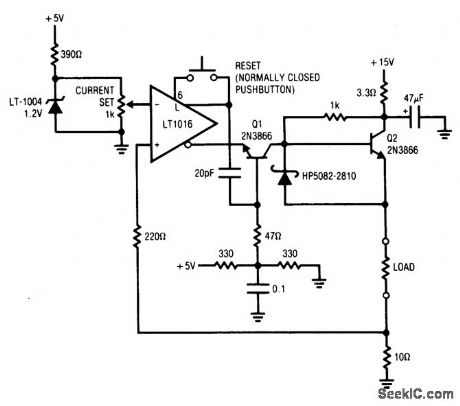
This circuit will turn off current in a load 12 ns after it exceeds a preset value. Under normal conditions the voltage across the 10 ohm shunt is smaller than the potential at the LT1016's negative input. This keeps Q1 off and Q2 receives bias, driving the load. When an overload occurs the current through the 10 ohm sense resistor begins to increase. When this current exceeds the preset value, the LT1016's outputs reverse.
This provides ideal turn-on drive for Q1 and it cuts off Q2 in 5 ns. The delay from the onset of excessive load current to complete shutdown is just 13 ns. Once the circuit has triggered, the LT1016 is held in its latched state by feedback from the non-inverting output. When the load fault has been cleared the pushbutton can be used to reset the circuit. (View)
View full Circuit Diagram | Comments | Reading(771)
HIGH_SPEED_ELECTRONIC_CIRCUIT_BREAKER
Published:2009/7/6 5:26:00 Author:May
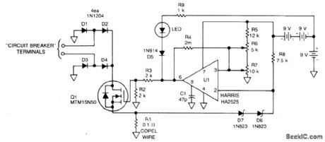
This 115 Vac, electronic circuit breaker uses the low drive power, low on resistance and fast turn off of the TMOS MTM15N50. The trip point is adjustable, LED fault indication is provided and battery power provides complete circuit isolation.
The two circuit breaker terminals are across one leg of a full wave diode bridge consisting of D1-D4. Normally, Q1 is turned ON so that the circuit breaker looks like a very low resistance. One input to comparator U1 is a fraction of the internal battery voltage and the other input is the drop across zeners D6 and D7 and the voltage drop across R1. If excessive current is drawn, the voltage drop across R1 increases beyond the comparator threshold (determined by the setting of R6), U1 output goes low, Q1 turns OFF, and the circuit breaker opens. When this occurs, the LED fault indicator is illuminated. (View)
View full Circuit Diagram | Comments | Reading(1256)
SAMPLE_AND_HOLD_CIRCUIT
Published:2009/7/6 5:25:00 Author:May
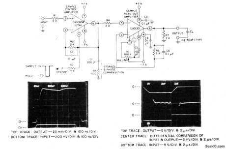
Circuit Notes
The circuit uses a CA3130 BiMOS op amp as the sample-readout amplifier for the storage (sample-holding) capacitor C1, and a CA3080A as the sample-control amplifler. Applications in linear systems to temporarily store analog data include DVM systems, industrial process-control, multiplex systems, and A-D converters. (View)
View full Circuit Diagram | Comments | Reading(882)
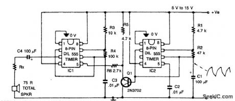
WARBLE_GENERATOR
Published:2009/7/6 5:25:00 Author:May
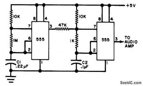
The circuit uses a pair of 555 timers or a single dual timer. Capacitor C1 controls the speed of the warble, while C2 determines the pitch. The values shown should produce quite a distinctive signal. (View)
View full Circuit Diagram | Comments | Reading(808)
9_V_BATTERY_LIFE_EXTENDER
Published:2009/7/6 5:24:00 Author:May
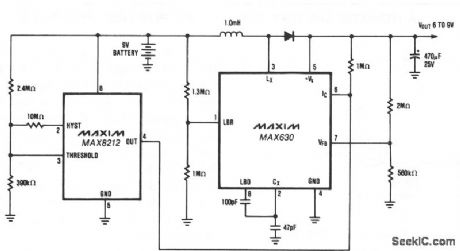
Circuit provides a minimum of 7 V until the 9-V battery voltage falls to less than 2 V. When the battery voltage is above 7 V, the MAX630's IC pin is low, putting it into the shutdown mode which draws only 10 nA. When the battery voltage falls to 7 V, the MAX8212 voltage detector's output increases. The MAX630 then maintains the output voltage at 7 V. The low battery detector (LBD) is used to decrease the oscillator frequency when the battery voltage falls to 3 V, thereby increasing the output current capability of the circuit. Note that this circuit, with or without the MAX8212, can be used to provide 5 V from 4 alkaline cells. The initial voltage is approximately 6 V, and the output is maintained at 5 V even when the battery voltage falls to less than 2 V. (View)
View full Circuit Diagram | Comments | Reading(801)
100_HZ_SQUARE_TRIANGLE
Published:2009/7/6 5:23:00 Author:May
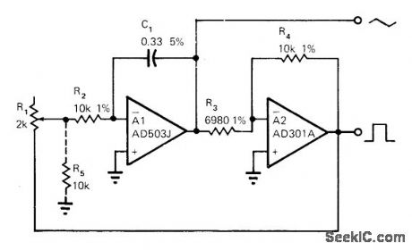
Two-opamp oscillatordelivers ±13 V square waves and ±10V triangle waves simultaneously at 100 Hz for values shown. By scaling R1, R2, and C1, wide range of frequencies can be covered down to o.1z (increase R2 to 10 megohms for frequencies near lower limit). Square-wave rise time is about 1.5 μs and fall time 0.5 μs. Opamp A1 operates as integrator and A2 as Schmitt trigger.-R. S. Burwen, Triangular and Square Wave Generator Has Wide Range, EDN Magazine, Dec. 1, 1972, p 59. (View)
View full Circuit Diagram | Comments | Reading(865)
NICAD_BATTERY_PROTECTION_CIRCUIT
Published:2009/7/6 5:23:00 Author:May
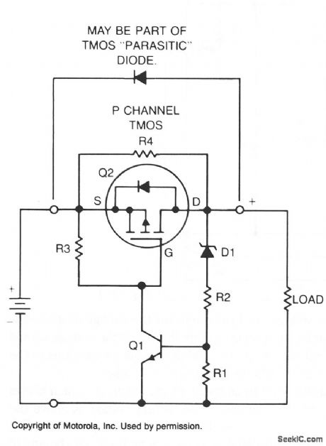
If a NiCad battery is discharged to a point at which the lowest capacity cell becomes fully discharged and reverses polarity, that cell will usually short internally and become unusable. To prevent this type of damage, this circuit detects a one-cell drop of 1.25 V and turns the load off before cell reversal can occur.
Low-current zener or other voltage sensor D1 and resistors R1 and R2 establish a reference level for transistor Q1. These resistors bias the zener to a few microamperes above its knee. Therefore, if battery voltage falls more than 1.25 V, Q1 turns off, turning off Q2, and disconnecting the load.After the load is disconnected, if the battery returns to nominal voltage, the high value of resistor shunting Q2 provides enough output voltage to reset the voltage sensor and tum Q2 back on. If desirable, shunt diode D2 or the parasitic diode of the TMOS device, if suitable, allows the battery to be charged from the load terminals.
The protection circuit presents a shunt current of only 10 mA at nominal battery voltage, which is low relative to the intemal leakage of the batteries. (View)
View full Circuit Diagram | Comments | Reading(1025)
5_MHz_VFO
Published:2009/7/6 5:23:00 Author:May
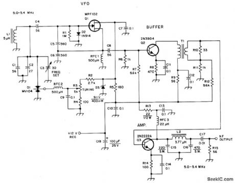
Circuit Notes
AJFET (Q1) serves as the oscillator. D2 helps to stabilize the transistor by limiting positive sinewave peaks and stabilizing the bias. Output from Q1 is supplied to a class A buffer, Q2. It operates as a broadband amplifter by means of T1, which is untuned. Output amplifter Q3 is also a class A stage. A low-pass, single-section ftlter is used at the output of Q3 to remove some of the harmonic currents generated within the system.The ftlter output impedance is 50 ohms. The injection level to the mixer is 600 mV p-p. (View)
View full Circuit Diagram | Comments | Reading(1198)
OVERVOLTAGE_PROTECTOR
Published:2009/7/6 5:22:00 Author:May
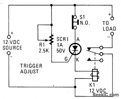
A silicon-controlled rectifier is installed in parallel with the 12-V line and connected to a normally-closed 12-V relay, K1. The SCR's gate circuit is used to sample the applied voltage. As long as the applied voltage stays below a given value, SCR1 remains off and K1's contacts remain closed, thereby supplying power to the load. When the source voltage rises above 12 V, sufficient current is applied to the gate of SCR1 to trigger it into conduction. The trigger point of SCR1 is dependent on the setting of R1. Once SCR1 is triggered (activating the relay), K1's contacts open, halting current flow to the load. (View)
View full Circuit Diagram | Comments | Reading(747)
AUTOMATIC_SHUTOFF_FOR_BATTERY_POWERED_PROJECTS
Published:2009/7/6 5:21:00 Author:May
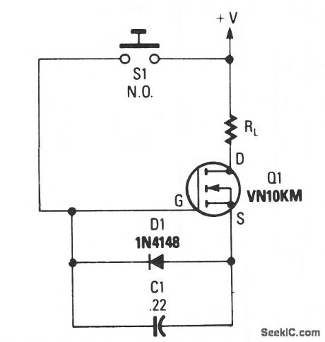
When S1 is depressed, C1 begins to charge to the supply voltage. That places a forward bias on the gate of Q1 turning it on and supplying current to load resistor RL. When the charge on C1 leaks off, the transistor shuts off, cutting off current to the load. That load could be anything from a transistor radio to a child's toy. Transistor Q1, available from Radio Shack as part No. 276-2070, is rated at 0.5 A at 60 Vdc. With a supply voltage of 9 Vdc and with C1 rated at 0.22 μF, a delay of about one minute is produced; with C1 rated at 10 μF, the delay is about an hour. (View)
View full Circuit Diagram | Comments | Reading(852)
ACCURATE_DIGITAL_CAPACITANCE_METER
Published:2009/7/6 5:20:00 Author:May
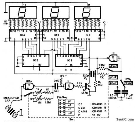
The principle of operation is counting the pulse number derived from a constant frequency oscillator during a fixed time interval produced by another lower frequency oscillator. This oscillator uses the capacitor being measured as the timing. The capacitance measurement is proportional during pulse counting during a fixed time interval. The astable oscillator formed by IC1c produces a pulse train of constant frequency. Gate IC1a also forms an oscillator whose oscillation period is given approximately by the equation: T=0.7 RC. Period T is linearly dependent on the capacitance C. This period is used as the time interval for one measurement. The differentiator network following the oscillator creates the negative spikes shaped in narrow pulses by IC1b NAND Schmitt Trigger. The differentiator formed by R1 and C1 produces a negative spike which resets the counters.The display shows the number of high frequency oscillator pulses entering the counter during the measurement period. (View)
View full Circuit Diagram | Comments | Reading(2811)
QUICKLY_DEACTIVATING_BATTERY_SENSOR
Published:2009/7/6 5:20:00 Author:May
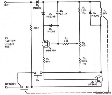
The sensing circuit rapidly disconnects the battery voltage and load whenever the voltage drops below a preset threshold. One-way operation prevents the circuit from reconnecting the load if the voltage should then rise above the threshold. C1 ensures that the circuit doesn't activate while making connections to the battery; if you accidentally reverse these connections, Dl will block the turn on the relay.
After you connect the battery, nothing happens until you depress pushbutton switch S1, which allows relay K1 to energize. When you release S1,,the relay remains on only if the battery voltage is above the minimum level. You preset this threshold-to 31.5 V when testing 36-V batteries, for example-using R4.Q1 begins to turn off as the battery voltage drops. Once the threshold level is reached, Q2 also begins to turn off, and its rising collector voltage provides positive feedback to the base of Q1, accelerating the turn off. When Q2 turns off, the relay drops out, disconnecting the battery from its load. (View)
View full Circuit Diagram | Comments | Reading(1075)
4W DC converter circuit composed of CW1524A
Published:2011/5/10 1:45:00 Author:Rebekka | Keyword: 4W DC converter
4W DC converter circuit composed of CW1524Ais shown as above. (View)
View full Circuit Diagram | Comments | Reading(705)
PROGRAMMABLE_ACTIVE_FILTERS
Published:2009/7/6 5:16:00 Author:May
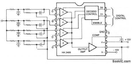
This is a second-order, low-pass filter with programmable cutoff frequency. This circuit should be driven from a low-source impedance since there are paths from the output to the input through the unse-lected networks. Virtually any filter function which can be constructed with a conventional op amp can be made programmable with the HA-2400.
A useful variation would be to wire one channel as a unity gain amplifier, so that one could select the unfiltered signal, or the same signal filtered in various manners. These could be cascaded to provide a wide variety of programmable filter functions. (View)
View full Circuit Diagram | Comments | Reading(1002)
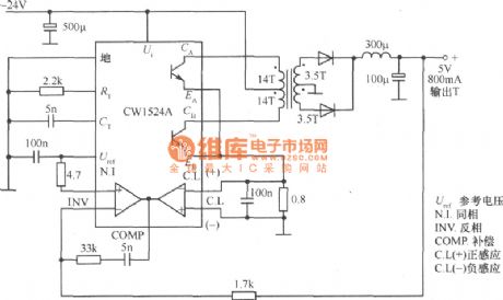
Half-bridge switching regulated power supply circuit composed of CW1524
Published:2011/5/10 1:44:00 Author:Rebekka | Keyword: Half-bridge switching regulated power supply

Half-bridge switching regulated power supply circuit composed of CW1524 is shown as above. (View)
View full Circuit Diagram | Comments | Reading(1247)
RESOLVER
Published:2009/7/6 5:14:00 Author:May

Circutt accepts DC input voltages R and X and generates two DC output voltages R sin X and R cos X. Can be used in guidance computers to solve coordinate conversion problems (polay to rectangular) and in feedback systems to convert rectangular to polar coordinate. Sine wave is generater by chopping input signalR and filtering resulting square wave. Sine wave is then samlpled at time controlled by X to generate R sin X. Cosine output is obtained by shifting first output 90oinphase.Circuit also generates proper sampling pulses and contains two sample-and-hold circuits on outPuts-W. H. Licata, Solid-State Resolver, EDN Magaz,ne, July 20, 1973, p 82-83. (View)
View full Circuit Diagram | Comments | Reading(1659)
FIELD_STRENGTH_METER
Published:2009/7/6 5:13:00 Author:May
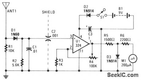
The untuned, but amplified FSM can almost sense that mythical flea's whisper-from 3 through 148 MHz no less-and yet, is so immune to overload that the meter pointer won't pin. The key to the circuit is the amplifter, a 324 quad op amp, of which only one section is used. It's designed for a single-ended power supply, will provide at least 20-dB dc gain, and the output current is self-limiting. The pointer can't be pinned. (View)
View full Circuit Diagram | Comments | Reading(0)
CAPACITANCE_TO_VOLTAGE_METER
Published:2009/7/6 5:09:00 Author:May

Timer U1 operates as a free-running oscillator at 60 Hz, providing trigger pulses to timer U2 which operates in the monostable mode. Resistor R1 is fixed and capacitor Cx is the capacitor being measured. While the output of U2 is 60 Hz, the duty cycle depends on the value of Cx. U3 is a combination low-pass filter and unity-gain follower whose dc voltage output is the time-averaged amplitude of the output pulses of U2, as shown in the timing diagram.
The diagram shows when the value of Cx is small the duty cycle is relatively low. The output pulses are narrow and produce a lower average dc voltage level at the output of U3. As the capacitance value of Ox increases, the duty cycle increases making the output pulses at U2 wider and the average dc level output at U3 increases. The graph illustrates capacitance values of 0.01 pF to 0.1 μF plotted against the output voltage of U3. Notice the excellent linearity and direct one-to-one scale calibration of the meter. If this does not occur the 100 k ohm resistor, R1, can be replaced with a potentiometer which can be adjusted to the proper value for the meter being used. (View)
View full Circuit Diagram | Comments | Reading(944)
| Pages:1044/2234 At 2010411042104310441045104610471048104910501051105210531054105510561057105810591060Under 20 |
Circuit Categories
power supply circuit
Amplifier Circuit
Basic Circuit
LED and Light Circuit
Sensor Circuit
Signal Processing
Electrical Equipment Circuit
Control Circuit
Remote Control Circuit
A/D-D/A Converter Circuit
Audio Circuit
Measuring and Test Circuit
Communication Circuit
Computer-Related Circuit
555 Circuit
Automotive Circuit
Repairing Circuit