
Circuit Diagram
Index 1058
Dc_coupled_tape_head_preamps_two_head
Published:2009/7/23 21:16:00 Author:Jessie
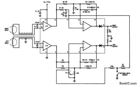
This circuit shows a dc-coupled, two-head stereo preamp using an LM1897. The circuit characteristics are: a GBW of 76 dB at 20 kHz, an S/N ratio of 62 dB (CCIR/ARM), distortion 0.03% at 1kHz, power-supply rejection greater than 95 dB, channel separation of60 dB, and a typical turn-on delay of 0.4 s. (View)
View full Circuit Diagram | Comments | Reading(2989)
Typical_guard_ring_layout_for_op_amps
Published:2009/7/23 21:16:00 Author:Jessie
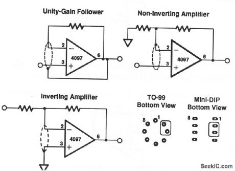
Even with properly cleaned and coated PC boards, leakage currents can limit the circuit performancc under severe environmental conditions. These currents can be intercepted before they reach the op-amp inputs by a guard ring or a conductor in the leakage path. The ring should surround the input terminals, and should be at the same potential as the inputs. Notice that the guard ring for the inverting and noninverting configurations connects to the inputs, while the unity-gain circuit connects to the output. (View)
View full Circuit Diagram | Comments | Reading(2652)
COMMUTATOR_SYNCHRONIZER
Published:2009/7/23 21:36:00 Author:Jessie
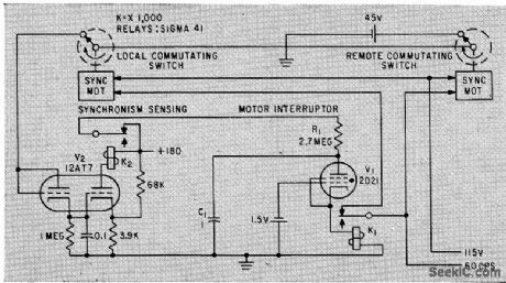
Automatic synchronizing circuit consists of motor interrupter and synchronism-sensing circuit. Commutator drive motor at control transmitter is interrupted until it syncs with commutator drive motor in robot that performs jobs in dangerous radioactive areas. Each interrupt makes motor drop bock 90°, so that only up to three interruptions are required to achieve synchronism.-D. A. Campbell, Multiplex Circuits for Control of a Robot, Electronics, 33;4, p 46-48. (View)
View full Circuit Diagram | Comments | Reading(1315)
Unity_gain_buffer
Published:2009/7/23 21:36:00 Author:Jessie
This configuration gives the highest input impedance of any op-amp circuit. Input impedance is equal to the differential input impedance multiplied by the open-loop gain, in parallel with common-mode input impedance. The gain error of this circuit is equal to the reciprocal of the open-loop gain or to the commonmode rejection, whichever is less. (View)
View full Circuit Diagram | Comments | Reading(1593)
Basic_noninverting_amplifier
Published:2009/7/23 21:35:00 Author:Jessie
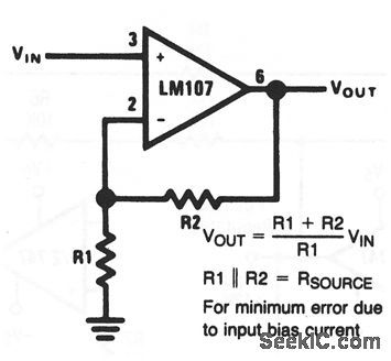
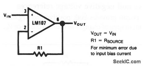
This circuit shows an LM107 that is connected in the classic noninverting amplifier configuration, where VOUT follows VIN The amplitude of the output depends on the ratio of R1 and R2 (within the limits of the supply voltage). The parallel resistance of R1 and R2 should equal the source resistance. (View)
View full Circuit Diagram | Comments | Reading(615)
50_V_PUSH_PULL_PULSES_FOR_DIODE_BRIDGE
Published:2009/7/23 21:35:00 Author:Jessie
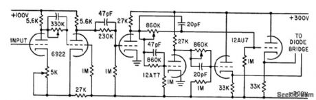
Schmitt trigger acts as comparator about 0 v and provides input to two pulse amplifiers. Cathode followers furnish push-pull output at low impedance necessary to drive a 6AL5 diode bridge. Permits two sampled-hold circuits to be run as memory pair in analog computer.-T. A. Brubaker, Precision Analog Memory has Extended Frequency Response, Electronics, 34:39, p 141-143. (View)
View full Circuit Diagram | Comments | Reading(1361)
555 Astable Oscillator Frequency and Duty Cycle Diagram for Quick Search
Published:2011/8/1 23:37:00 Author:Zoey | Keyword: 555 astable oscillator frequency, duty cycle diagram, quick search

The circuit diagram and waveform of the astable multi-vibrator have been shown in picture 3-1.THey can be calculated according to the following formula:
f=1.433/(Ra+2Rb)C
D=t1/t=(Ra+Rb)/(Ra+2Rb)
In order to simplify, speed up, and convenience the procedure of debugging and designing the circuit, the relationship curve series between multi-vibrator’s oscillation and frequency f(Hz), capacitance C(μF) and (RA+2Rb)(Ω)has been illustrated in picture 3-2(a); The relationship curve series between time resistance, Ra, Rb and duty cycle has been shown in picture 3-2(b). (View)
View full Circuit Diagram | Comments | Reading(1084)
Low_cost_supervisory_circuit_high_reliability_manual_reset
Published:2009/7/23 21:35:00 Author:Jessie
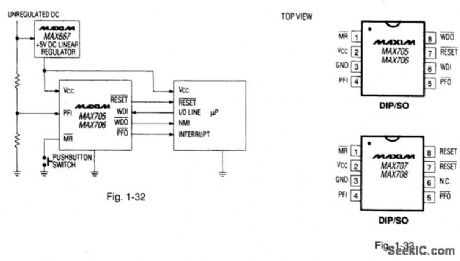
Figures 1-32 and 1-33 show a typical application circuit and pin configurations, respectively, for the MAX705-708. The ICs are similar to that described for Figs. t-J through 1-M, but with generally lower cost. The ICs have a 200-ms reset pulse width, 200-p, A quiescent current, and a 1.25-V threshold detector for power-fail warning, low-battery detection, or for monitoring a power supply other than +5 V.The MAX705/MAX707 generate a reset pulse when the supply is below 4.65V. The MAX706/708 generate a reset below 4.4V. The MAX707/708 is the same as the MAX705/706, except an active-high reset is substituted for the watchdog timer.The watchdog is activated when the WDI input has not been toggled within 1.6 s. MAXIM HIGH-RELIABILITY DATA Book, 1993, P. 5-31. (View)
View full Circuit Diagram | Comments | Reading(913)
Low_noise_low_power_amplifier
Published:2009/7/23 21:34:00 Author:Jessie
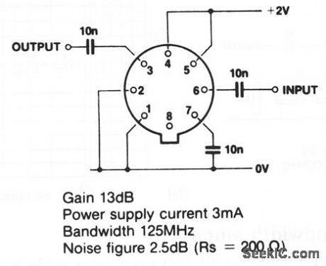
This circuit shows an SL560 used as a low-noise, low-power consumption amplifier. (View)
View full Circuit Diagram | Comments | Reading(658)
COURTESY_LIGHT_DELAY_SWITCH
Published:2009/7/6 2:15:00 Author:May
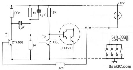

This circuit holds on the internal light for approximately one minute after the car doors are closed. When the door contacts open, a + VE pulse is applied to the base of T1. This transistor turns on, turning off T2 and charging the 10-μF capacitor. T3 turns on, holding on the intemal light . The capacitor takes one minute to discharge when the circuit reverts to its original state. (View)
View full Circuit Diagram | Comments | Reading(811)
General_digital_IC_troubleshooting_tips
Published:2009/7/23 21:21:00 Author:Jessie
The following troubleshooting tips apply to digital circuits where the majority of components are contained in ICs.
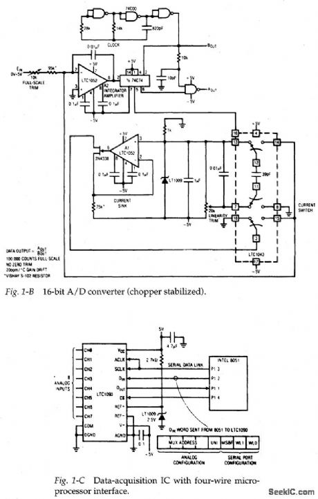
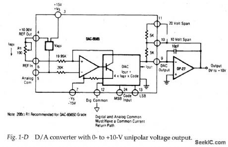
Power and ground connectionsThe first step in tracing problems in a digital circuit with ICs is to check all power and ground connections to the ICs. Many ICs have more than one power and one ground connection. For example, the LTC1043 in Fig. 1-B requires +5 V at pins 4 and 5, and -5 V at pin 17. Also, the LTC1090 in Fig. 1-C has both a digital ground (DGND) and an analog ground (AGND). Likewise, the DAC-8565 in Fig. 1-D has both an analog common (pin 5) and a digital common (pin 12).
With all power and ground connections confirmed, check that all the ICs receive reset, chip-select, start, and any other function signals, as required. For example, the DAC-4881 in Fig. 1-E requires a chip-select signal at pin 1, as well as address-decode signals at pins 2 and 28. Likewise, the ADC0808/080 in Fig. 1-F requires start, ALE, EOC, and output-enable signals from the microprocessor or control logic. If any of these signals are absent or abnormal (incorrect amplitude, improper timing, etc.) circuit operation comes to an immediate halt.In some cases, control signals to digital ICs are pulses (usually timed in a certain sequence) and other control signals are steady (high or low). If any of the lines carrying the signals to the ICs are open, shorted to ground, or to power (typically +5 V or +12 V, and 3 V or 3.3 V for newer digital circuits), the IC will not function. So, if you find an IC control pin that is always high, always low, or apparently is connected to nothing (floating), check the PC traces or other wiring to that pin carefully.As an example, when the DAC4881 is connected as a 12-bit straight-binary digital-to-analog converter (Chapter 6) as shown in Fig. 1-G, the chip-select (pin 1) and address-decode (pins 2, 28) are connected to ground. If the DAC4881 is connected as an 8-bit with complementary input DAC (Fig. 1-E), the chip-select must receive a write (WR) signal, and the address-decode pins must receive address bits from the microprocessor.
(View)
View full Circuit Diagram | Comments | Reading(1144)
DUAL_CONVERSION_SYNTHESIZER
Published:2009/7/6 2:15:00 Author:May
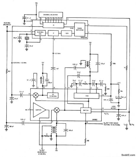
Singlecrystal transceiver system uses 10.240-MHz reference frequency which is added to VC0 frequency to produce transmit frequency. Same 10.240-MHz reference frequency is mixed with first IF signal to generate 455-kHz second IF signal. Dividing reference by 2 provides 5.120-MHz signal that is lightly coupled to multiply-by-3 buffer whose output is tuned to third harmonic (15.360 MHz). This is mixed with VCO frequency to provide input signal for programmable divider, When VCO is operating as first mixer and local oscillator on CB channel 1 (16.270 MHz), difference frequency is 910 kHz. Programmable divider divides by 182 to give necessary 5-kHz input to phase detector. If VCO moves off frequency, divided input to phase detector moves away from 5 kHz and action of loop pulls VC0 back on frequency.-L. Sample, A Linear CB Synthesizer, IEEE Transactions on Consumer Electronics, Aug. 1977, p 200-206. (View)
View full Circuit Diagram | Comments | Reading(867)
Minimum_component_audio_amplifier
Published:2009/7/23 21:21:00 Author:Jessie
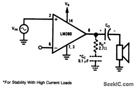
Because the LM380 has internal biasing and compensation, this basic audio amplifier requires only an output-coupling capacitor (typically 500μF). Of course, such an amplifier has no tone- or volume-control (Figs. 1-33 through 1-36).The circuit can supply about 2.5 W into an 8-Ω speaker, with a VS of 12V or greater. The RC and CC components suppress 5- to 10-MHz oscillation that can occur during the negative swing into a high-current load. Although such oscillation will not pass through the speaker, the radiated signals can produce interference in RF-sensitive equipment. (View)
View full Circuit Diagram | Comments | Reading(1527)
10_1_PRESCALER_FOR_500_MHz
Published:2009/7/6 2:14:00 Author:May
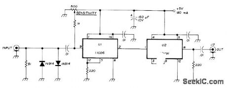
Uses Fairchild 11C06 D flip-flop and Fairchild 95H91 divide-bp 5 counter. Input sensitivity is less than 100 mV from 10 to 500 MHz. Back-to-back diodes protect 11C06 input from overloads. Output is fed to 50-MHz frequency counter. Use regulated supply.-W, C. Ryder, 500-MHz Decade Prescaler, Ham Radio, June 1975, p 32-33. (View)
View full Circuit Diagram | Comments | Reading(2319)
Composite_high_speed_precision_amplifier
Published:2009/7/23 21:21:00 Author:Jessie
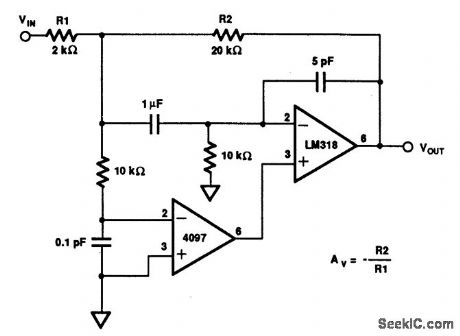
This circuit provides a gain of 10 with the values shown. (View)
View full Circuit Diagram | Comments | Reading(836)
Operation principle of 555 estable multi-vibrator model
Published:2011/7/30 3:06:00 Author:Zoey | Keyword: 555, Astable Multi-vibrator, Model
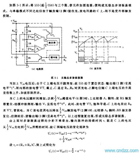
As shown in the picture 3-1, an astable multi-vibrator can be formed after connecting a 555, three resistances and a capacity accessory, the trigger (pin 2) is connected on loop C.
When galvanized voltage VDD, 555 will be reset and pin 3 will havehigh level “1”, the discharge tube VT1 will cease to discharge, and C will get charged via Ra and Rb.
Voltage on C increases along with time, when it gets 2/3 VDD threshold value level, the upper comparator A1 will turn over, RS trigger willset and output a low level”0”, at that time, the discharge tube VT1 will be saturated and conducted, electric charge on C will discharge through Rb to VT1. When C discharges to 1/3 VDD, the upper comparator A2 will turn over, RS trigger willreset and output a high level”1”, this process will be repeated many times.
By analyzing the results, we can conclude that the change rule of voltage on the two terminals of C can be formulated as follow:
Uc(t)=VDD(1-e-t(RA+RB)C)
+1/3 VDDE-t(RA+RB)C
If we replace (RA+RB) with t1, the formula can be simplified as follow:
Uc(t)=VDD(1-2/3•e-t/t1)
Following formula can be concluded:
T=0.693(RA+2RB)C
D=t1/T=(RA+RB)/(RA+2RB)
If RA>>RB, then D≈50%, the output oscillation wave is square wave.
finally we can draw following conclusions:
(1) The oscillation period is not relevant to VDD, but is determined by charge and discharge time constant, that is, the value of RA, RB, and C
(2) Duty cycle of the oscillation is not relevant to C , but is relevant to the ratio of RA and RB
(View)
View full Circuit Diagram | Comments | Reading(1145)
TRANSIENT_REJECTING_SCR_TRIGGER
Published:2009/7/23 21:21:00 Author:Jessie
Integrator combined with voltage comparator detects difference in voltage-time areas of data pulses and random transients. Dotc pulses passed are 8 v high and 0.5 millisec wide.-S. B. Marshall, Noise-Rejecting SCR Trigger Circuit, EEE, 14:7, p 102-104. (View)
View full Circuit Diagram | Comments | Reading(765)
Z80_interface_with_partial_decoding_for_A_D_converter
Published:2009/7/23 21:20:00 Author:Jessie
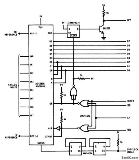
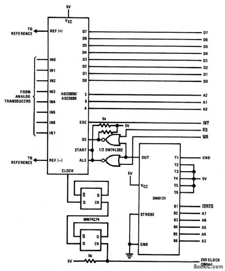
This circuit shows a Z80 interface for the ADC0808/0809 where the DM8131 decodes 5 address bits and the IOREQ I/O request strobe. Two NOR gates gate the RD and WR strobes for ALE, START, and OE inputs. (View)
View full Circuit Diagram | Comments | Reading(1181)
Microphone_preamp_with_low_supply_voltage
Published:2009/7/23 21:20:00 Author:Jessie
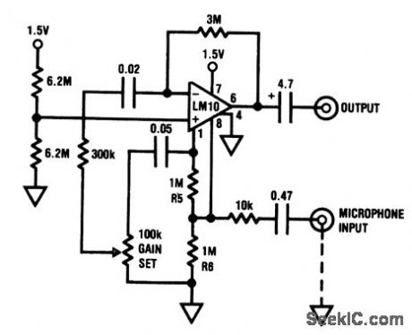
This preamp operates from a single 1.5-V cell, and can be located rightat the microphonQ. The circuit has 60-dB gain with a 10-kHz bandwidth, unloaded, and 5-kHz bandwidthwhile loadedwith 500Ω.The input impedance is10 kΩ. (View)
View full Circuit Diagram | Comments | Reading(856)
TRIGGER_FOR_ANY_INPUT
Published:2009/7/23 21:27:00 Author:Jessie

D-c coupling of input permits triggering either by sine waves or pulses, independently of pulse shape or rise time.-P. L. Writer, DC Input Trigger Circuit,EEE,10:9,p 29. (View)
View full Circuit Diagram | Comments | Reading(698)
| Pages:1058/2234 At 2010411042104310441045104610471048104910501051105210531054105510561057105810591060Under 20 |
Circuit Categories
power supply circuit
Amplifier Circuit
Basic Circuit
LED and Light Circuit
Sensor Circuit
Signal Processing
Electrical Equipment Circuit
Control Circuit
Remote Control Circuit
A/D-D/A Converter Circuit
Audio Circuit
Measuring and Test Circuit
Communication Circuit
Computer-Related Circuit
555 Circuit
Automotive Circuit
Repairing Circuit