
Circuit Diagram
Index 1043
THREE_PHASE_CLOCK_FROM_AREFERENCE_CLOCK
Published:2009/7/6 5:35:00 Author:May
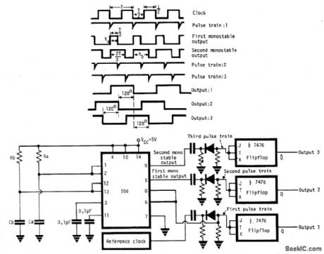
The circuit provides three square wave outputs with 120' of phase difference between each other. Reference clock frequency is twice that of the required frequency. This can be obtained from a crystal oscillator with a chain of dividers or by using LM555 in 50% duty cycle astable mode. If1/T is the frequency of the reference clock, the dual timer 556 is connected to give two mono-stable output pulses of duration T/3 and 2T/3. The first timer R and C value are adjusted so that ta 1.1RaCa = T/3 and the second timer R and C values so that tb = 1.1RbCb =2T/3. For triggering the two monostables a negative pulse train (1st) is derived from the reference clock with a differentiator and a clipper combination as shown. The three pulse trains trigger three JK flip flops giving three phase square wave outputs. (View)
View full Circuit Diagram | Comments | Reading(1387)
LOW_POWER_ACTIVE_FILTER_WITH_DIGITALLY_SELECTABLE_CENTER_FREQUENCY
Published:2009/7/6 5:34:00 Author:May
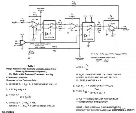
The switchable center frequency active filter allows a decade change in center frequency. (View)
View full Circuit Diagram | Comments | Reading(762)
Low_distortion_bridge_audio_power_amplifier
Published:2009/7/23 21:09:00 Author:Jessie
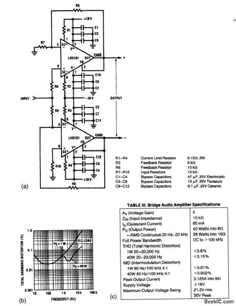
This circuit is capable of 40-W into an 8-Ω speaker, or 28-W into a 16-Ω speaker, with a voltage gain of 3 and a full-power bandwidth from dc to 100 kHz. Figures 1-44B and 1-44C show the circuit performance characteristics. (View)
View full Circuit Diagram | Comments | Reading(863)
Commercial power safe voltage protector circuit diagram
Published:2011/8/2 2:43:00 Author:Rebekka | Keyword: Commercial power safe voltage protector
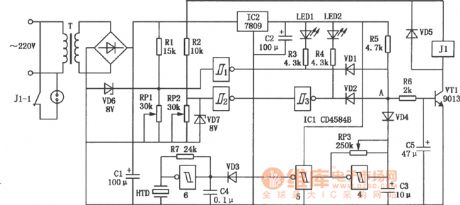
The protector can cut off the power supply automatically and and issue intermittent alarm sound and lighting instructions when the main power protector is lower or higher than the set voltage. The circuit plays the role of automatic protection for household appliances. (View)
View full Circuit Diagram | Comments | Reading(1305)
MULTIFUNCTION_SIREN_SYSTEM
Published:2009/7/6 5:32:00 Author:May
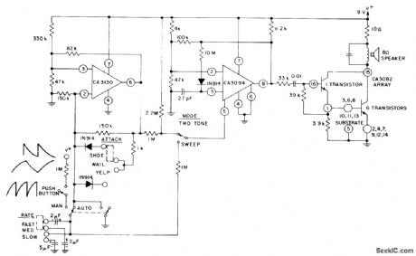
The circuit uses a CA3130 BiMOS op amp as a multivibrator to control the siren's rate. A CA3094 used as a VCO is followed by a CA3082 transistor array used to drive a speaker. A Manual or Auto mode switch allows the user to select either intermittent or continuous siren operation, respectively. In addition, three switches are available that control Mode , Attack , and Rate .
(View)
View full Circuit Diagram | Comments | Reading(1644)
20_KC_TRIGGER_GENERATOR
Published:2009/7/23 21:09:00 Author:Jessie
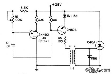
Uses ujt to drive 2N526 transistor from cutoff to saturation. Since energy in C1 is not used to trigger ser, small capacitor can be used, thereby increasing operating frequency limit.- Transistor Manual, Seventh Edition, General Electric Co., 1964, p 333. (View)
View full Circuit Diagram | Comments | Reading(785)
ELECTRONIC_CROWBAR
Published:2009/7/6 5:31:00 Author:May
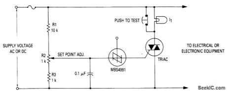
Where it is desirable to shut down equipment rather than allow it to operate on excessive supply voltage, an electronic crowbar circuit can be employed to quickly place a short-circuit across the power lines, thereby dropping the voltage across the protected device to near zero and blowing a fuse. Since the TRIAC and SBS are both bilateral devices, the circuit is equally useful on ac or dc supply lines. With the values shown for R1, R2 and R3, the crowbar operating point can be adjusted over the range of 60 to 120 volts dc or 42 to 84 volts ac. The resistor values can be changed to cover a different range of supply voltages. The voltage rating of the TRIAC must be greater than the highest operating point as set by R2. I1 is a low power incandescent lamp with a voltage rating equal to the supply voltage. It may be used to check the set point and operation of the unit by opening the test switch and adjusting the input or set point to fire the SBS. (View)
View full Circuit Diagram | Comments | Reading(1910)
Wideband_amplifier_for_test_equipment_applications
Published:2009/7/23 21:09:00 Author:Jessie
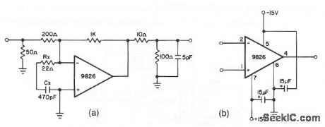
This circuit shows a 9826 used in an application where high speed at a relatively low gain is required (a gain of 5 in this case). Rx and Cx form a lead/lag network between the inverting and noninverting inputs. With the values given, this circuit can operate comfortably at frequencies of 20 MHz. If a lower gain is needed (gain less than 5), connect a 1- to 5-pF capacitor between the output and inverting input to aid in suppressing parasitic oscillations. The 100-Ω 5-pF filter at the output has a damping effect to help suppress signal overshoot. Figure 3-54B shows external connections for the 9826. (View)
View full Circuit Diagram | Comments | Reading(733)
WARBLING_TONE_GENERATOR
Published:2009/7/6 5:31:00 Author:May
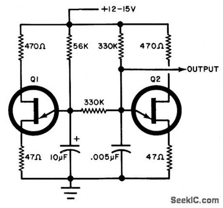
The circuit use two unijunction transistors. The low-frequency sawtooth generated by Q1 modulates the high-frequency tone generated by Q2. The output should feed into a high-impedance amplifier. Q1 = Q2 = 2N4871.
(View)
View full Circuit Diagram | Comments | Reading(1059)
Wideband_difference_amplifier
Published:2009/7/23 21:08:00 Author:Jessie
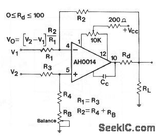
This circuit shows an AH0014 connected as a basic differential or instrumentation amplifier with a balance adjustment. The balance resistor is adjusted for best common-mode rejection ratio. Figure 3-48B shows external connections for the AH0014. (View)
View full Circuit Diagram | Comments | Reading(783)
LINE_DROPOUT_DETECTOR
Published:2009/7/6 5:30:00 Author:May
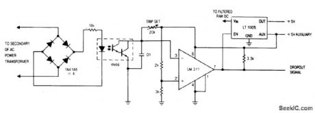
View full Circuit Diagram | Comments | Reading(771)
6800_polled_interface_for_A_D_converter
Published:2009/7/23 21:07:00 Author:Jessie

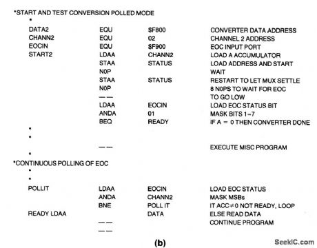
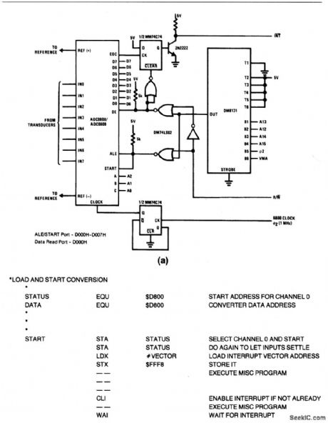

This circuit shows a 6800 polled I/O interface for the ADC0808/0809, with full address decoding. Figure 6-26B shows typical polled routines. (View)
View full Circuit Diagram | Comments | Reading(1303)
FAST,PRECISION_SAMPLE_HOLD
Published:2009/7/6 5:30:00 Author:May
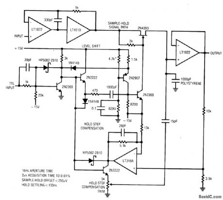
View full Circuit Diagram | Comments | Reading(617)
WARBLE_TONE_ALARM
Published:2009/7/6 5:30:00 Author:May
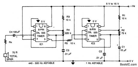
The circuit generates a warble-tone alarm signal that simulates the sound of a British police siren. IC1 is wired as an alarm generator and IC2 is wired as a 1 Hz astable multivibrator. The output of IC2 is used to frequency modulate IC1 via R5. The action is such that the output frequency of IC1 alternates symmetrically between 500 Hz and 440 Hz, taking one sound to complete each alternating cycle. (View)
View full Circuit Diagram | Comments | Reading(1880)
Port_address_structure_to_where_channel_is_a_separate_address
Published:2009/7/23 20:48:00 Author:Jessie


With this configuration, each channel of the ADC (Fig.6-20) looks like the same address. (View)
View full Circuit Diagram | Comments | Reading(658)
AUTOMATIC_POWER_DOWN_PROTECTION_CIRCUIT
Published:2009/7/6 5:30:00 Author:May
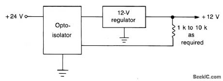
This circuit is faster than a fuse and automatically resets itself when a short is removed. The normal regulated dc input line is opened and the phototransistor of the opto isolator is connected in series with the source and regulator. Between the output of the regulator and ground is a LED and an associated current-limiting resistor, placed physically close to the surface of the photosensitive device. As long as the regulator is delivering its rated output, the LED glows and causes the photo device to have a low resistance. Full current is thus allowed to flow. If a short circuit occurs on the output side of the regulator, the LED goes dark, the resistance of the photo device increases, and the regulator shuts off. When the short is removed, the LED glows, and the regulator resumes operation. (View)
View full Circuit Diagram | Comments | Reading(806)
Port_address_structure_where_channel_is_selected_by_3_bit_word
Published:2009/7/23 20:47:00 Author:Jessie

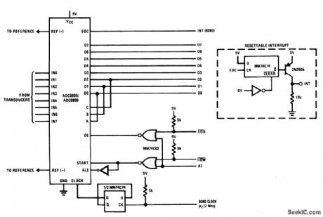
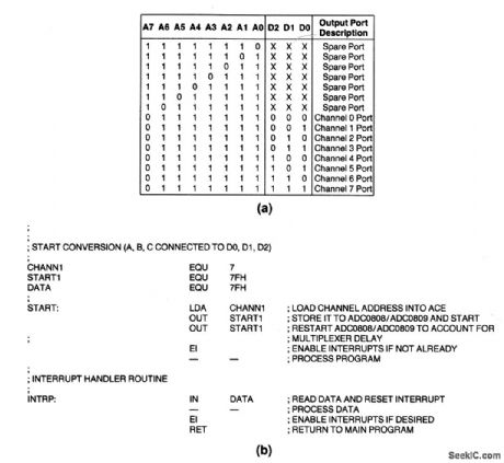
With this configuration, the ADC (Fig.6-20) looks like a port address where the channel is selected by the 3-bit status word written on the data bus. Figure 6-21 B shows a typical interrupt I/O routine. (View)
View full Circuit Diagram | Comments | Reading(605)
BIQUAD_AUDIO_FILTER
Published:2009/7/6 5:30:00 Author:May
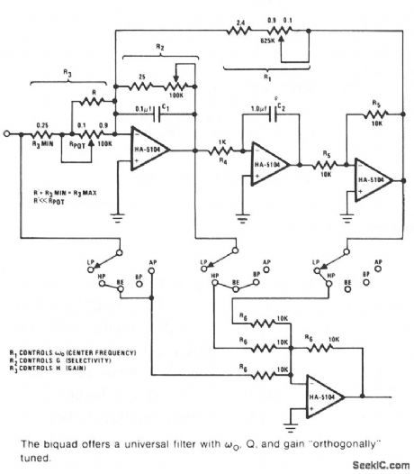
This universal ftlter offers low-pass, high-pass, bandpass, band elimination, and all-pass functions.The Biquad consists of two successive integration stages followed by an inverting stage. The entire group has a feedback loop from the front to the back consisting of R1 which is chiefly responsible for controlling the center frequency, ωo. The first stage of integration is a poor integrator because R2 limits the range of integration. R2 and C form the time constant of the first stage integrator with R3 influencing gain H almost directly. The band-pass function is taken after the ftrst stage with the lowpass function taken after the third stage. The remaining ftlter operations are generated by various combinations of three stages.
The Biquad is orthogonally tuned, meaning that ωo. Q. and gain H can all be independently adjusted. The component values known will allow ωo, to range from 40 Hz to 20 kHz. The other component values give an adequate range of operation to allow for virtually universal filtering in the audio region. ωo Q. and gain H can all be independently adjusted by tuning R1 through R3 in succession. (View)
View full Circuit Diagram | Comments | Reading(1004)
High_speed_low_VSUBOS_SUB_composite_amplifter
Published:2009/7/23 20:36:00 Author:Jessie
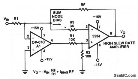
This circuit combines an OP-07C and a 5534 to form a high-speed amplifier with low output offset voltage. Notice that VO depends primarily on RF and R1. (View)
View full Circuit Diagram | Comments | Reading(1329)
LOW_VOLTAGE_POWER
Published:2009/7/6 5:29:00 Author:May
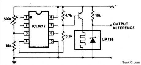
There are some classes of circuits that require the power supply to be disconnected if the power supply voltage falls below a certain value. As an example, the National LM199 precision reference has an on chip heater which malfunctions with supply voltages below 9 volts causing an excessive device temperature. The ICL8212 can be used to detect a power supply voltage of 9 volts and turn the power supply off to the LM199 heater section below that voltage. (View)
View full Circuit Diagram | Comments | Reading(824)
| Pages:1043/2234 At 2010411042104310441045104610471048104910501051105210531054105510561057105810591060Under 20 |
Circuit Categories
power supply circuit
Amplifier Circuit
Basic Circuit
LED and Light Circuit
Sensor Circuit
Signal Processing
Electrical Equipment Circuit
Control Circuit
Remote Control Circuit
A/D-D/A Converter Circuit
Audio Circuit
Measuring and Test Circuit
Communication Circuit
Computer-Related Circuit
555 Circuit
Automotive Circuit
Repairing Circuit