
Circuit Diagram
Index 1050
TACHOMETER_WITH_SET_POINT
Published:2009/7/6 3:28:00 Author:May
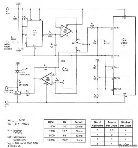
View full Circuit Diagram | Comments | Reading(1315)
Log_amplifier
Published:2009/7/23 20:24:00 Author:Jessie

Compare this op-amp circuit to the log-amplifier circuits of chapters 2 and 3.
(View)
View full Circuit Diagram | Comments | Reading(0)
DIVIDE_BY_5_WITH_TWO_GATES_AND_3_BITS
Published:2009/7/6 3:28:00 Author:May
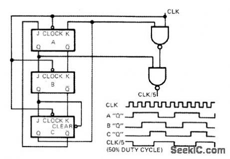
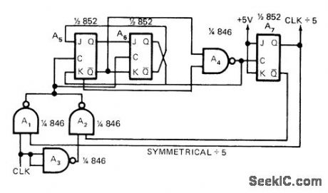
Arrangement shown for dlviding clock inputfrequency by 5 requires onlytwo gates from 846 IC and 3 bits of 852 JK flip-flop storage to glve square-wave output pulses having 50% duty cycle.-C,L,Maginnlss, Another Reader Respondsto Odd Modulo Dlvider,EDN Magazine,Oct,15,1972,p 57. (View)
View full Circuit Diagram | Comments | Reading(780)
Precision_high_speed_op_amp_for_video_applications
Published:2009/7/23 20:24:00 Author:Jessie
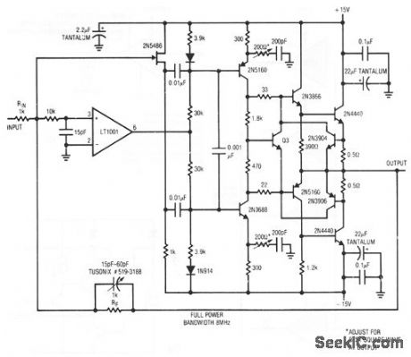
This circuit features a 1500-V/μs slew rate, full output to 8 MHz, ±10-V drive into a 10-Ω load, and is short-circuit protected at ± 1 A. RF layout techniques and a ground plane are mandatory, and the 2N4440s must have heatsinks. The 200-Ω resistors are adjusted for best square-wave output. The 15- to 60-pF peaking-capacitor adjustment should be optimized under loaded output conditions.
(View)
View full Circuit Diagram | Comments | Reading(1048)
SYMMETRICAL_DIVIDE_BY_5_CLOCK
Published:2009/7/6 3:27:00 Author:May
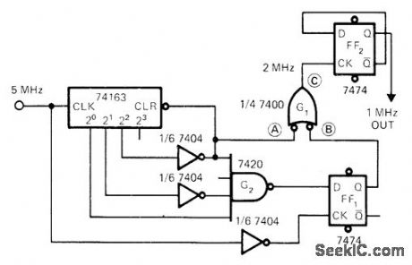
Uses 74163 counter to generate two phases of 1-MHz clock pulse with 50% duty cycle from 5-MHz system reference. One phase is decode of binary 4 from counter, while other is decode of 1 clocked at midbit time. Both phases are recombined in gate G1 to give 2-MHz clock that toggles FF2 to generate desired 1-MHz output.-L. A.Mann, Divider Circuit Maintains Pulse Symmetry, EDN Magazine, July 1, 1972, p 54-55. (View)
View full Circuit Diagram | Comments | Reading(1001)
10_MHz_FRONT_END
Published:2009/7/6 3:25:00 Author:May
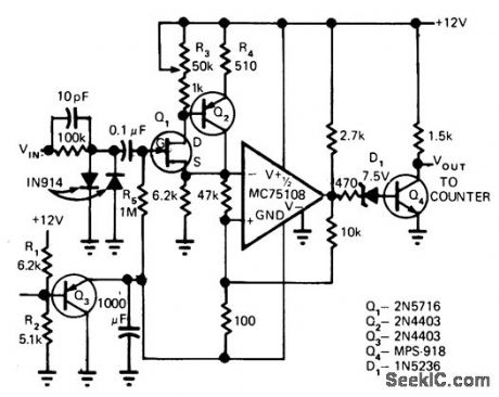
Front-end design for battery-operated 5-MHz counter consists of FET and bipolar buffer followed by Schmitt trigger made from MC75108 dual line receiver. Circuit operates linearly upto 10 MHz with 25-mV input signal. Requires swings from logic 0 (0 V) to logic 1(about 10 V), for which suitable counter circuit is given in article. Accepts any input waveform shape and level.-D. Aldridge, CMOS Counter Circuitry Slashes Battery Power Requirements, EDN Magazine, Oct. 20, 1974, p 65-71. (View)
View full Circuit Diagram | Comments | Reading(800)
Precision_current_sink
Published:2009/7/23 20:22:00 Author:Jessie
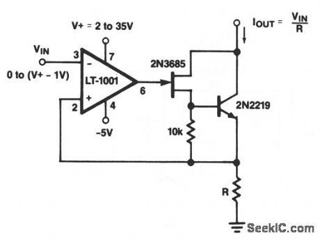
As shown, the ability of this circuit to sink current depends on VIN and the value of R. Note that VIN can be anything from 0 to (V + - 1 V), and V+ can be +2 to +35 V. (View)
View full Circuit Diagram | Comments | Reading(1)
Boosted_gain_amplifier
Published:2009/7/23 20:22:00 Author:Jessie
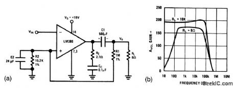
For applications that require gains higher than the internally set gain of 50, it is possible to apply positive feedback around the LM380 for closed-loop gains of up to 300. As shown in Fig. 1-41B, this circuit has a gain of about 200 (well beyond the audio range) when the load is 10 kΩ. When the load is a typical 8-Ω speaker, the circuit provides a gain of over 170 (beyond the audio range). (View)
View full Circuit Diagram | Comments | Reading(1341)
12_BIT_BINARY_2s_COMPLEMENT_D_A_CONVERSION_SYSTEM
Published:2009/7/6 3:25:00 Author:May
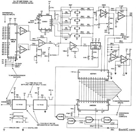
The front end of the DAC is configured differentially using dual eight-input IC multiplexer 1H6216 and three LM156 op amps. Following the differential amplifier is the programmable gain stage discussed earlier, with a low-pass filter on the output feeding the IH5110 sample and hold amplifier. The output of the IH5110 is connected to the comparator input, - input LM301, through the internal10-KΩ feedback resistor of the 7541 multiplying d/a converter. The AD7541, along with a ±10-V reference and successive approximation logic, make up the 2's complement a/d converter. (View)
View full Circuit Diagram | Comments | Reading(2057)
ZERO_HYSTERESIS_SCHMITT
Published:2009/7/23 20:46:00 Author:Jessie
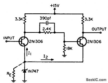
Turn-on and turn-off voltages are made identical by using zener diode in place of RE.-R. A. Wilson, Zero-Hysteresis Schmitt Trigger, EEE, 13:2, p 62. (View)
View full Circuit Diagram | Comments | Reading(726)
PROGRAMMABLE_COUNTER
Published:2009/7/6 3:23:00 Author:May
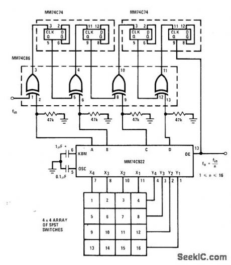
Input frequency can be divided by any number between 1 and 16 by pressing appropriate key on keyboard connected to National MM74C922 16-key encoder. Output frequency is symmetrical for odd and even divisors. Can be used for simple frequency synthesis or as keyboard-controlled CRO trigger. Operates over standard CMOS supply range of 3-15 V. Typical upperfrequency limit is 1 MHzwith 10-V supply. Circuit uses two MM74C74 dual D flip-flops and MM74C86 EX-CLUSIVE-OR package.- CMOS Databook, National Semiconductor, Santa Clara, CA, 1977, p 5-50-5-51.
(View)
View full Circuit Diagram | Comments | Reading(2248)
EMITTER_TRIGGERED_FLIP_FLOP
Published:2009/7/23 20:45:00 Author:Jessie
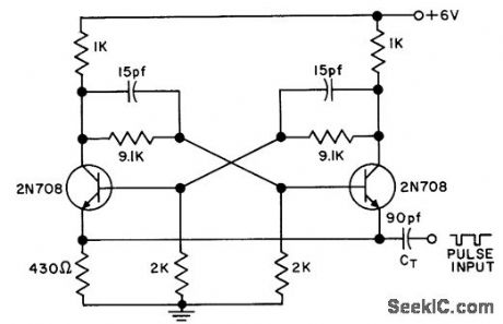
Pulse input, makes alternate sides of flip-flop conduct on alternate trigger pulses. Maximum trigger rate exceeds 2 Mc with trigger amplitude from 4 to 12 v. Chief limitation is high trigger current required.- Transistor Manual, Seventh Edition, General Electric Co., 1964, p 196. (View)
View full Circuit Diagram | Comments | Reading(730)
TR_CIRCUIT
Published:2009/7/6 3:23:00 Author:May
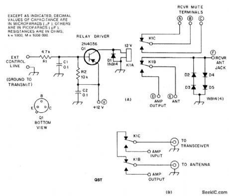
Circuit Notes
C1 and C2 are disc ceramic. R1 and R2 are 1/4 or 1/2 W carbon composition resistors. K1 is a 12 V DPDT DIP relay. Illustration A shows how to connect the relay contacts for use with a separate transmitter-receiver combination. The circuit at B is for amplifier use with a transceiver. (View)
View full Circuit Diagram | Comments | Reading(748)
SOUARE_WAVE_DIVIDER
Published:2009/7/6 3:22:00 Author:May
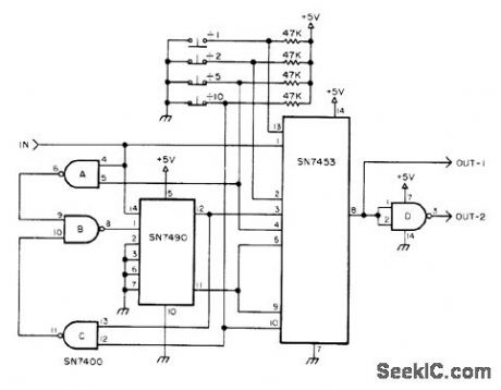
Divides input square wave by 1, 2, 5, or 10 depending on which switch is open. Signal at OUT-1 is inverted with respect to input, and OUT-2 is noninverted.-Circuits, 73 Magazine, June 1977, p 49. (View)
View full Circuit Diagram | Comments | Reading(834)
Basic_8080_8224_8228_interface_for_A_D_converter
Published:2009/7/23 20:43:00 Author:Jessie
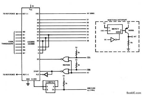
This circuit shows a minimum-component interface for the ADC0808/ 0809, where the EOC is tied directly to the 8080 interrupt input. If an INS8228 is used and the INTA pin is tied through a 1-kΩ resistor, the interrupt will cause a restart, RST, to be executed. This causes a jump to a restart vector, and execution of the interrupt. If a very simple multi-interrupt system is desired, a wired-OR configuration using resetable latches (as shown in dashed lines) can be used. Figures 6-21 and 6-22 show the I/O port-address structures. (View)
View full Circuit Diagram | Comments | Reading(1172)
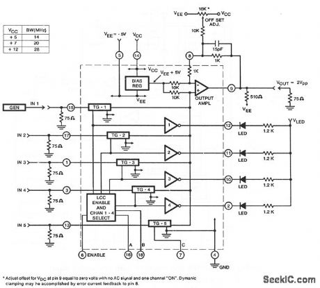
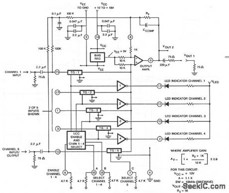
8_to_1_video_switch_amplifier
Published:2009/7/23 20:43:00 Author:Jessie

This circuit uses two CA3256 ICs to provide an 8-to-1 video-switch function. The analog switches of channels 1 to 8 are digitally controlled by logic, as shown in the truth table. As in the case of the switch circuits shown in Figs. 3-35 through 3-37, the circuit of Fig. 3-38 has programmable gain for all channels, as well as flexible output-voltage swing. Typically, the output voltage swing can be about 5 Vpp, with a Vcc to VEE range of 12 V or greater, and each amplifier can provide a gain of 1 into a 75-Ω load, or a gain of 5 into a 1-kΩ load. (View)
View full Circuit Diagram | Comments | Reading(1085)
DIVIDE_BY_5
Published:2009/7/6 3:20:00 Author:May
Requires only two digital chip types, Input clock is alternately inverted and noninverted for clocking divide-by-3 counter, to give effect of dividing by 21/2 which toggles A3 to give symmetrical divide-by-5 output with 50% duty cycle for pulses. Article gives timing diagram and traces operation of circuit.-C. W.Hardy, Reader Responds to Odd Modulo Divider in July 1st EDN, EDN Magazine, Oct. 1, 1972, p 50. (View)
View full Circuit Diagram | Comments | Reading(2337)
Analog_video_switch_and_amplifier_with_direct_coupled_input_and_output
Published:2009/7/23 20:42:00 Author:Jessie
This circuit shows a CA3256 switch/amplifier connected for a direct-coupled input and output. One of four channels can be selected in parallel with channel 5. The analog switches of channels 1 to 4 are digitally controlled by logic (Fig. 3-35B). A VEE of -5 V is required. The peak-to-peak output voltage is fixed by the Vcc and VEE range, and is about +3.6 to -2.5 V (clipped) for a Vcc of +5 V and a VEE of -5 V. For a 2-Vpp output, Vcc must be +4V, and VEE must be -4 V. This produces a bandwidth of about 10 MHz. Higher Vcc produces greater bandwidths, as shown. (View)
View full Circuit Diagram | Comments | Reading(831)
TRIAC_RELAY_CONTACT_PROTECTION
Published:2009/7/6 3:19:00 Author:May
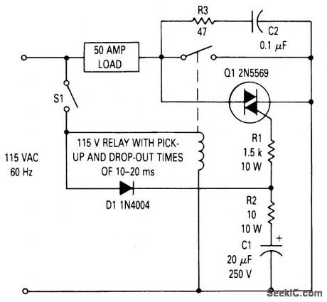
Circuit Notes
This circuit can be used to prevent relay contact arcing for loads up to 50 amperes.There is some delay between the time a relay coil is energized and the time the contacts close. There is also a delay between the time the coil is de-energized and the time the contacts open. For the relay used in this circuit both times are about 15 ms. The TRIAC across the relay contacts will turn on as soon as sufficient gate current is present to fire it. This occurs after switch S1 is closed but before the relay contacts close. When the contacts close, the load current passes through them, rather than through the TRIAC, even though the TRIAC is receiving gate current. If 51 should be closed during the negative half cycle of the ac line, the TRIAC will not turn on immediately but will wait until the voltage begins to go positive, at which time diode Dl conducts providing gate current through R1. The maximum time that could elapse before the TRIAC turns on is 8-1/3 ms for the 60 Hz supply. This is adequate to ensure that the TRIAC will be on before the relay contact closes. (View)
View full Circuit Diagram | Comments | Reading(1356)
Analog_video_switch_and_amplifier_with_ac_coupled_input
Published:2009/7/23 20:40:00 Author:Jessie
This circuit shows a CA3256 switch/amplifier connected for an ac coupled input. One of four channels can be selected in parallel with channel 5. The analog switches of channels 1 to 4 are digitally controlled by logic (Fig. 3-35B).Vcc can be from + 12 to + 18 V.VEE is grounded, Amplifier gain is determined by external resistor Rf, as shown by the equation. A typical value of CCOMP is 6 pF. (View)
View full Circuit Diagram | Comments | Reading(796)
| Pages:1050/2234 At 2010411042104310441045104610471048104910501051105210531054105510561057105810591060Under 20 |
Circuit Categories
power supply circuit
Amplifier Circuit
Basic Circuit
LED and Light Circuit
Sensor Circuit
Signal Processing
Electrical Equipment Circuit
Control Circuit
Remote Control Circuit
A/D-D/A Converter Circuit
Audio Circuit
Measuring and Test Circuit
Communication Circuit
Computer-Related Circuit
555 Circuit
Automotive Circuit
Repairing Circuit