
Circuit Diagram
Index 1053
Unity_gain_inverting_wideband_amplifier
Published:2009/7/23 20:57:00 Author:Jessie
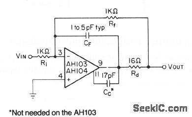
This circuit shows the basic connections in a typical unity-gain inverting amplifier. The use of a compensation capacitor Cc is required for the AN104, unless the gain is fairly high. The AN103 only needs additional external compensation in special cases, such as when used as a noninverting unity-gain follower. Rd in the output circuit improves frequency stability. CF compensates for a pole in the closed-loop transfer function, caused by the input capacitance and feedback resistors. A ground plane is recommended, leads must be short, and Rf should not exceed 5.6 kΩ. Typical bandwidth is 35 MHz, with slew rates of 230 V/μs, into a 330-Ω load (View)
View full Circuit Diagram | Comments | Reading(920)
Ac_coupled_video_amplifier_with_single_supply
Published:2009/7/23 20:56:00 Author:Jessie
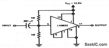
This circuit can be used in ac applications, such as video amplifiers and active filters, but requires only one supply. The output swing is over 8 Vpp with a 12-V supply. Input impedance is about 500 kΩ. (View)
View full Circuit Diagram | Comments | Reading(700)
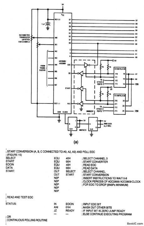
8080_8224_8228_interrupt_type_interface_for_A_D_converter
Published:2009/7/23 20:56:00 Author:Jessie
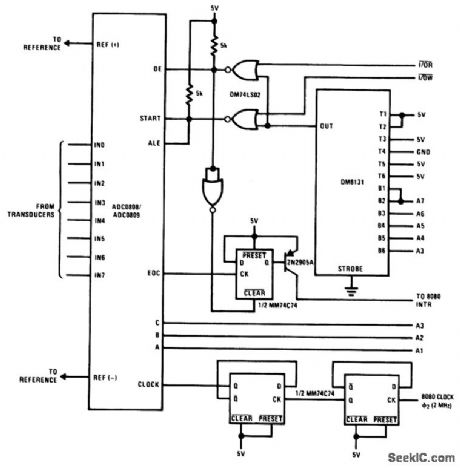
This circuit shows an interrupt-type interface for the ADC0808/0809 using a 6-bit bus comparator to decode a read-and-write strobe. Viewed from the CPU, this interface looks like a bidirectional data port where the address is set by the logic levels on the in inputs of the DM8131. When data bits are written to the ADC, the 3 least-significant bits on the address bus define the channel to be converted. The rest of the bits are decoded to provide the START and ALE strobes (Fig. 6-13B). When the conversion is completed, EOC sets the interrupt flip-flop, and (when the data bits are read) the interrupt is complete. (View)
View full Circuit Diagram | Comments | Reading(1742)
Ac_coupled_video_amplifier_with_high_input_impedance
Published:2009/7/23 20:55:00 Author:Jessie
This circuit can be used in ac applications, such as in video amplifiers and active filters. The circuit uses boot-strapping to achieve input impedances in excess of 10 MΩ. (View)
View full Circuit Diagram | Comments | Reading(641)
Mitsubishi Pajero light off-road vehicle power window wiring circuit diagram(Continued)
Published:2011/5/10 0:52:00 Author:Rebekka | Keyword: Light off-road vehicle , power window, Mitsubishi Pajero
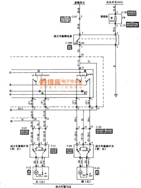
Mitsubishi Pajero light off-road vehicle power window wiring circuit diagram(Continued) is shown as above. (View)
View full Circuit Diagram | Comments | Reading(2993)
VOLTAGE_SENSING_TRIGGER
Published:2009/7/23 20:55:00 Author:Jessie
Long-term stability is better than 10 mv, and can be improved still more by adding two silicon diodes in series with R2. Ideal for use in go-no-go applications.- Transistor Manual, Seventh Edition, General Electric Co., 1964, p 325. (View)
View full Circuit Diagram | Comments | Reading(714)
Mitsubishi Pajero light off-road vehicle power windows wiring circuit diagram
Published:2011/5/10 1:03:00 Author:Rebekka | Keyword: Mitsubishi Pajero , light off-road vehicle power
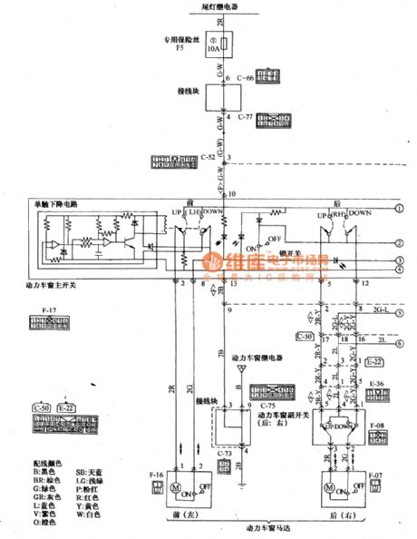
Mitsubishi Pajero (PAJERO) light off-road vehicle power windows wiring circuit diagram is shown as above.
Wiring color:B: black SB: light blue BR: brown LG: light green G: green P: pink GR: grey R: red L: blue Y: yellow V: purple W: white O: orange
(View)
View full Circuit Diagram | Comments | Reading(3485)
DIVIDER_WITH_PULSE_SHAPER
Published:2009/7/6 3:07:00 Author:May

Hah of Exar XR-2556 dual timer divides input pulse frequency by 2 or 3, and other haff shapes output pulse by controlling duty cycle over range that can be adjusted from 1% to 99% with R,. Supply voltage can be 4.5-16 V.- Timer Data Book, Exar Integrated Systems, Sunnyvale, CA, 1978, p 23-30. (View)
View full Circuit Diagram | Comments | Reading(726)
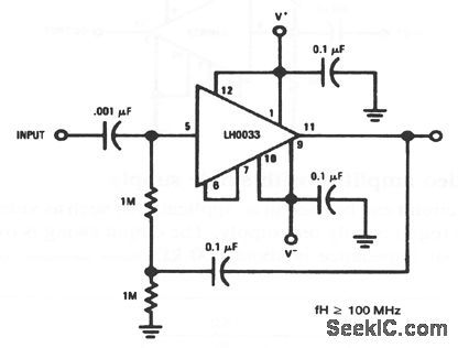
Shield_or_line_driver_for_high_speed_video_applications
Published:2009/7/23 20:54:00 Author:Jessie
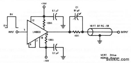
This circuit uses the low input current, high speed, and high-capacitance drive capabilities of the LH0033 to full advantage for high-speed video applications, such as in automatic test equipment. In this circuit, the LH003 is. mounted close to the device under test, and drives the cable/shield, thus allowing higher-speed operation because the device under test does not have to charge the cable. (View)
View full Circuit Diagram | Comments | Reading(654)
5_20_V_ZENER_STABILIZED
Published:2009/7/6 3:06:00 Author:May
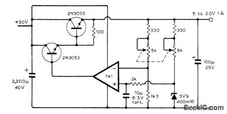
Use of dual linear pot simplifies problem of feeding reference zener diode from variable-voltage supply.-L.J Baughan, Vatiable Power Supply with Zener Stabilization, Wireless World, Nov. 1975、p 520 (View)
View full Circuit Diagram | Comments | Reading(730)
DIVIDER_FOR_7_MHz
Published:2009/7/6 3:05:00 Author:May
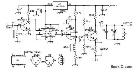
Used after 7-MHz VFO of 40-meter transmitter, to provide 3.5 MHz as required for operation in 80-meter band. Half of 7474 TTL D flip-flop Un is connected in divide-by-2 configuration. U2 provides required well-regulated 5-V source. Q1 clips negative-going portion of 7-MHz sine wave to prevent damage to 7474. Square-wave 3.5-MHz output from U1 is applied to source-follower Q2 which drives class A amplifier output stage Q3. RFC1 and RFC2 are 10 μH. C1 is 6.8-μF 10-V tantalum. Q2 is 100-pF mica. L1 is 41 turns No. 26 enamel spaced to fill entire 7-80-2 core,to give 10 ptH.-S. Creason, A VFO Frequency Divider, QST, Nov. 1976, p 23-24.
(View)
View full Circuit Diagram | Comments | Reading(2274)
8080_8224_8228_Polled_interface_for_A_D_converter
Published:2009/7/23 20:54:00 Author:Jessie

This circuit shows a polled interface for the ADC0808/0809.where the address is partially decoded by a DM74LS139, which creates the read and write strobes to operate the ADC. The circuit can be connected in an interrupt mode using resettable latches (as shown in the dashed lines of Fig. 6-20). Figure 6-23B shows typical polled routines. (View)
View full Circuit Diagram | Comments | Reading(619)
Mitsubishi Pajero light-weight off-road vehicle headlamp scrubber wiring circuit diagram
Published:2011/5/10 1:00:00 Author:Rebekka | Keyword: Mitsubishi Pajero , light-weight off-road vehicle
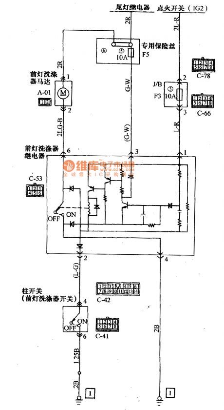
Mitsubishi Pajero light-weight off-road vehicle headlamp scrubber wiring circuit diagram is shown as above. (View)
View full Circuit Diagram | Comments | Reading(2105)
AF_DlVlSlON_BY_2_TO_11
Published:2009/7/6 3:03:00 Author:May
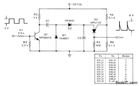
Ratio of C2 to C1 determines division ratio, as given in table. When C2 charges to peak point firing voltage of Q2, it fires and discharges C2, so C1 charges to line voltage. Q2 then turns off. Next cycle begins with another positive pulse on base of Q1, discharging C1. Division range can be chanced by utilizing programmable aspect of PUT Q2 and changing ratio of resistances.-R. J. Haver and B. C. Shiner, Theory, Characteristics and Applications of the Programmable Unijunetion Transistor, Motorola, Phoenix, AZ, 1974 AN-S27, p 9. (View)
View full Circuit Diagram | Comments | Reading(727)
JFET_bipolar_cascode_video_amplifier
Published:2009/7/23 20:51:00 Author:Jessie
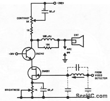
This cascode circuit provides full video output for the CRT cathode drive. Gain is about 90. The cascode configuration eliminates Miller-capacitance problems with the JFET, thus allowing direct drive from the video detector. An m-derived filter, which uses stray capacitance and a variable inductor, prevents a 4.5-MHz sound frequency from being amplified by the video amplifier. (View)
View full Circuit Diagram | Comments | Reading(0)
DIVIDING_40_60_MHz_BY_2_3_OR_4
Published:2009/7/6 3:01:00 Author:May
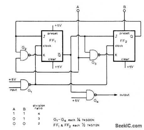
Division ratio is controlled externally by making control terminals A and B high (1) or low (0), as given in table. Developed for use in receiver requiring local oscillator covering 10 to 30 MHz. Counter simplifies tuner design.-C. Attenborough, Fast Modulo-3 Counter, Wireless World, Aug. 1976,p 52. (View)
View full Circuit Diagram | Comments | Reading(896)
LOW_LEVEL_THRESHOLD_DETECTOR
Published:2009/7/23 20:51:00 Author:Jessie
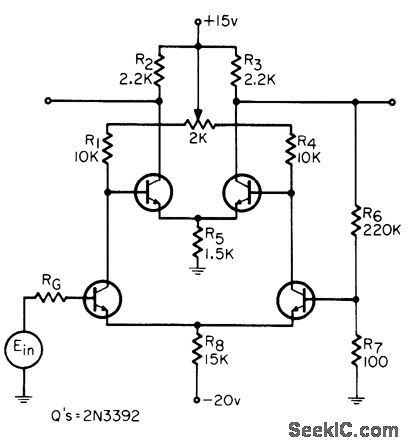
Determines when millivolt-range signal exceeds adjustable threshold. Circuit is similar to Schmitt trigger. Forward gain of amplifier is increased by adding second differential amplifier stage having two low-cost transistors and three resistors. Hysteresis can be as low as 2 mv, as compared to 100 mv in standard Schmitt.-R. M. Muth, Stable Threshold Circuit With Low Hysteresis, EEE, 14:1, p 64. (View)
View full Circuit Diagram | Comments | Reading(1002)
WIDE_BANDWIDTH_PEAK_DETECTOR
Published:2009/7/6 3:00:00 Author:May
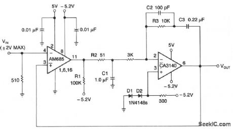
This circuit can detect the positive peaks for signal frequencies higher than 5 MHz. It yields ±1% accuracy for 400 mV to 4 V pk-pk signal amplitudes on sine, square, and triangular waveforms. The Am685 comparator output increases whenever VIN is a greater negative voltage than VOUT; the high comparator output, in turn, charges C1 in a positive direction. The CA3140 op amp amplifies the C1 voltage with respect to the ECL-switching-threshold voltage (- 1.3 V) developed by diodes D1 and D2. For repetitive waveforms, each cycle boosts VOUT until it equals the peak input value. The peak-detection process is aided by the comparator's open-emitter output, which allows C1 to charge rapidly through R2, but to discharge slowly through R2 and R1. Reducing the value of C1 shortens system-response times. Although the circuit can't detect negative-going peaks, it can be modified to measure the pk-pk value of bipolar signals that are symmetric about ground. To do so, divide VOUT by 2 using two 1-KΩ resistors and feed the comparator VOUT/2 rather than VOUT. (View)
View full Circuit Diagram | Comments | Reading(1210)
DIVIDE_BY_9_WITH_SHIFT_REGISTER
Published:2009/7/6 2:59:00 Author:May
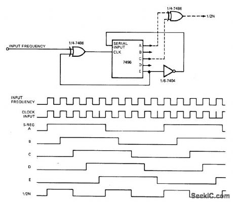
Uses 7496 as 5-bit shift register,7486 as EXCLUSIVE-OR gate,and 7404 as inverter to give division of square-, aveinput frequency by 9 while main-taining 50% duty cycle at output Article covorsconnection changes needed for other divisionratios,With 8-bit shiftregister,circuit, divideby as much as 15,Addition of,486 EXCLUSIVE-OR gate across any outputs,as shown by dashed lines,makes effective output har that of basic TTL circuit,-J,N,Hobbs,Jr.,Divide-by-N Uses Shift Register,EDN Magazine,Oct 5,1976,p 108.
(View)
View full Circuit Diagram | Comments | Reading(2303)
DIVIDE_BY_7
Published:2009/7/6 2:58:00 Author:May
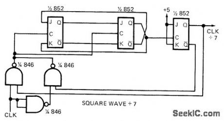
Requires only two differenttypes of chips. Input clock is alternately inverted and noninverted by gates operating in conjunction with 3 bits of storage using 852, to give squarewave output at one-seventh of clock frequency.-C. W. Hardy, Reader Responds to Odd Modulo Divider in July 1st EDN, EDN Magazine, Oct. 1, 1972, p 50. (View)
View full Circuit Diagram | Comments | Reading(766)
| Pages:1053/2234 At 2010411042104310441045104610471048104910501051105210531054105510561057105810591060Under 20 |
Circuit Categories
power supply circuit
Amplifier Circuit
Basic Circuit
LED and Light Circuit
Sensor Circuit
Signal Processing
Electrical Equipment Circuit
Control Circuit
Remote Control Circuit
A/D-D/A Converter Circuit
Audio Circuit
Measuring and Test Circuit
Communication Circuit
Computer-Related Circuit
555 Circuit
Automotive Circuit
Repairing Circuit