
Circuit Diagram
Index 1052
TWO_PHASE_VOLTAGE_CONTROLLED
Published:2009/7/6 3:09:00 Author:May

Produces fixed-amplitude sawtooth outputs that can be shaped to give sine waves, with outputs of the two identical channels differing by a specified phase such as 90o. Each output is integrated to give rising or falling ramp that controls switching FET of opposite channel. With oscillation established, one integrator output goes toward zero and the other away from zero, with same or opposite polarity. When first output crosses zero, discriminator switches FET in input amplifier of other channel, witch action being self-perpetuating to give desired sawtooth outputs. Dashed-line gating at outputs of discriminators can be used to boost slope of one sawtooth in one quadrant.-F. B. Jones, Voltage-Controlled Two-Phase Sawtooth Oscillator, Wireless World, June 1973, p 285. (View)
View full Circuit Diagram | Comments | Reading(707)
71_65V_AT_0_1_A
Published:2009/7/6 3:09:00 Author:May
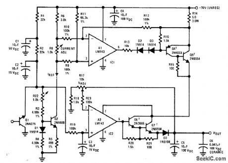
Provides continuously variable output voltage and adjustable output cur-rent range. Q1 is connected as zener to give 6.5-V reference voltage. Darlington current boosters Q4-Q7 should be on common Thermafloy 60068 or equivalent heatsink. Developed for use with pulsed loads. For input volt-age range of 46-76 V, regulation is within 286 mV for 500-mA DC output.- Linear Applica-tions, Vol. 2, National Semiconductor, Santa Clara, CA, 1976, AN-127, p 8-10. (View)
View full Circuit Diagram | Comments | Reading(684)
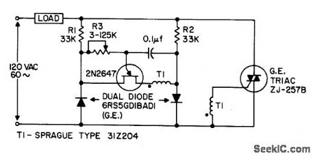
FAST_RECOVERY_COLLECTOR_TRIGGERING
Published:2009/7/23 21:06:00 Author:Jessie
Additional diode, used in place of resistor from midpoint of diode pair to +6 v, has high back impedance to prevent shunting of trigger pulse during triggering period, and has low forward impedance to insure fast recovery. - Transistor Manual, Seventh Edition, General Electric Co., 1964, p 198. (View)
View full Circuit Diagram | Comments | Reading(624)
Mitsubishi Pajero light off-road vehicle central control door lock set (continued) wiring circuit diagram
Published:2011/5/10 1:07:00 Author:Rebekka | Keyword: Central control door lock set , Mitsubishi Pajero, light off-road vehicle
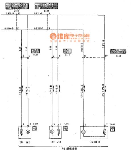
Mitsubishi Pajero light off-road vehicle central control door lock set (continued) wiring circuit diagram is shown as above.
Wiring Color B: Black LG: light green G: Green L: Blue W: White Y: Yellow SB: sky blue BR: Brown 0: Orange GR: Gray R: red P:Pink V: Purple (View)
View full Circuit Diagram | Comments | Reading(2008)
Noninverting_amplifier_for_gains_greater_than_10
Published:2009/7/23 21:05:00 Author:Jessie
This circuit shows an AH0014 connected as a noninverting wideband amplifier, where gains must be greater than 10. The characteristics are the same as for the circuit of Fig. 3-49. Figure 3-48B shows external connections for the AH0014. (View)
View full Circuit Diagram | Comments | Reading(603)
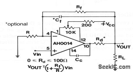
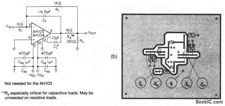
Inverting_amplifier_for_gains_greater_than_10
Published:2009/7/23 21:04:00 Author:Jessie
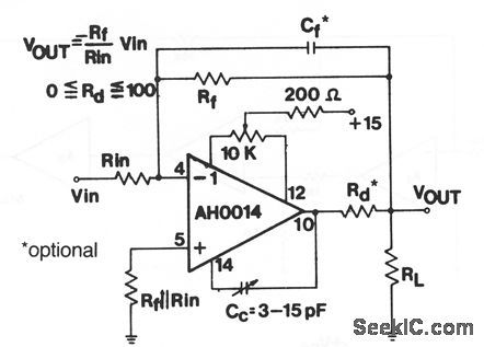
This circuit shows an AH0014 connected as an inverting wideband amplifier, where gain must be greater than 10. If the gain is over 100, Cc can generally be omitted. For best results, use an Rf of 1 kΩ or less (to minimize the effects of stray capacitance). When Cc is in the 10-pF range, a stable gain of 20 dB is possible at 10 MHz. If peaking occurs, tower Cc to the 1- to 5-pF range. Atypical value for CF (when used) is 1 to 5 pF. A typical value for Rd (when used) is 33Ω.Figure 3-48B shows external connections for the AH0014. (View)
View full Circuit Diagram | Comments | Reading(715)
_15_V_FROM_HIGH_INPUT_VOLTAGE
Published:2009/7/6 3:08:00 Author:May
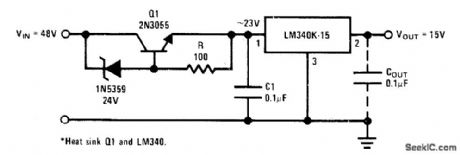
Zener is used in series with resistor R to level-shift input voltage higher than rated maximum of LM340K-15 regulator. Typical load regulation is 40 mV for 0-1 A pulsed load, and line regulation is 2 mV for 1-V change in input voltage for no load.With optional output capacitor, circuit noise is only 700 ptV P-P.- Linear Applications, Vol. 2, National Semiconductor, Santa Clara, CA, 1976, AN-103,p9-10. (View)
View full Circuit Diagram | Comments | Reading(1686)
Composite_amplifier_with_current_boost
Published:2009/7/23 21:03:00 Author:Jessie
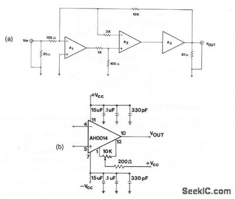
In this circuit, A1 is used to improve the dc characteristics of A2, which, in turn, determines the bandwidth of A3. Using an OP-07 for A1, an AH0014 for A2, and an AH0010 for A3, the circuit is capable of driving a 51-Ω load at±5 V to 10 MHz. Drift is less than 1μV/℃ with an offset of 20 μV. Figure 3-48B shows the external connections for the AH0014. (View)
View full Circuit Diagram | Comments | Reading(639)
6800_interface_with_partial_address_decoding_for_A_D_converter
Published:2009/7/23 21:02:00 Author:Jessie
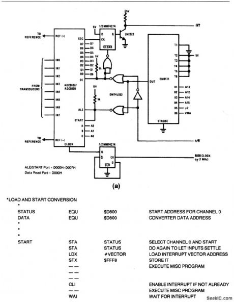

This circuit shows a typical6800 interrupt interface for the ADC0808/ 0809 using a flip-flop and an open-collector transistor. The interrupt is reset when the data bits are read. Figure 6-25B shows routine. (View)
View full Circuit Diagram | Comments | Reading(1262)
High_speed_fast_settling_pulse_amplifier
Published:2009/7/23 21:01:00 Author:Jessie
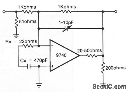
In this circuit, the amplifier is set for unity gain. The input signal is terminated into 51Ω. This resistance, together with the 470-pF capacitor, compensates for stray capacitances that might appear at the input. With the values shown (and the variable capacitor adjusted to 5 pF), the output is± 10 V swing at ±50-mA drive current, with unity gain up to 100 MHz (assuming a typical ± 15-V supply. The pin connections are: 1 output, 10 +Vcc, 11-Vcc, 16-input, 19 +input, 20 common. (View)
View full Circuit Diagram | Comments | Reading(867)
TRANSIENT_ATTENUATING_TRIGGER
Published:2009/7/23 21:01:00 Author:Jessie

Transformer coupling and diode bridge between ujt and scr greatly attenuate transients, to prevent premature triggering of ujt when used for impulse commutation in d-c choppers and invertors.- Transistor Manual, Seventh Edition, General Electric Co., 1964, p 333. (View)
View full Circuit Diagram | Comments | Reading(597)
CURRENT_SENSING
Published:2009/7/23 20:50:00 Author:Jessie
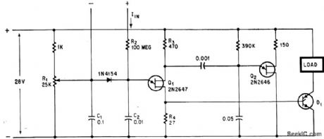
Input current of only 40 no will charge C2 and raise voltage at emitter of Q1 to triggering level. C1 and C2 then discharge through R4, und resulting generating pulse triggers scr D1 in series with load. Recovery is rapid.-D. V. Jones, Quick-On-The-Trigger Design, Electronics, 38:12, p 105-110. (View)
View full Circuit Diagram | Comments | Reading(1469)
TV_video_IF_amplifier_and_synchronous_detector_for_cable_receivers
Published:2009/7/23 20:50:00 Author:Jessie
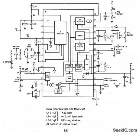
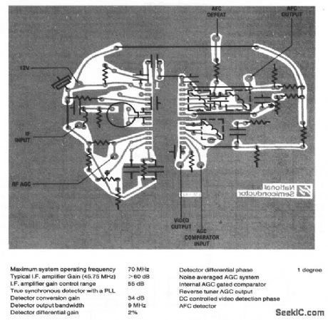
This circuit shows the external connections for an LM1823, which is a video IF amplifier that is designed to operate at intermediate carrier frequencies up to 70 MHz, and use phase-locked loops (PLLs) for synchronous detection of amplitude modulation on these carrier frequencies. Figure 3-39B shows a typical PC layout, and Fig .3-39C tabulates the circuit characteristics. (View)
View full Circuit Diagram | Comments | Reading(837)
DUAL_TIMER_TONE_STEPPER
Published:2009/7/6 3:08:00 Author:May
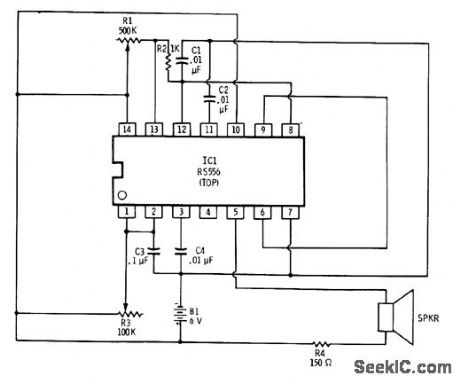
One section of RS556 dual timer is connected as free-running astable MVBR for supplying pulses to trigger input of other section connected as mono MVBR driving loudspeaker. When both MVBRs are adjusted so one trigger pulse initiates each timing period and no trigger pulses occur during timing pefiods, output tone has frequency of freerunning MVBR. With two trigger pulses per timing cycle, every other trigger pulse is ignored and tone is at half frequency. With three trigger pulses per cycle, output is one-third of frequency. Can be used for classloom demonstration of electronic music;settings of R1 and R3 can be adjusted to give tones regembling violin, bagpipes, or almost any other instrument.-F. M. Mims, Integrated Circuit Projects, Vol. 6, Radio Shack, Fort Worth, TX, 1977, p 70-78. (View)
View full Circuit Diagram | Comments | Reading(647)
HUM_FREE_CASSETTE_RECORDER_SUPPLY
Published:2009/7/6 3:08:00 Author:May
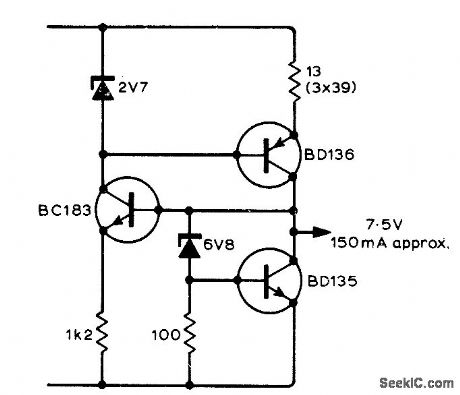
Designed for tape recorder feeding into AF amplifier, to permit operation of recorder from power supply of amplifier without having hum due to positive feedback through shared ground connection. Circuit provides up to 150 mA at 7.5 V from supply ranging from 12 to 24 V. Transistors are connected as constant-currentsource in series with constant-voltage sink.Use three39-ohm resistors in parallel as 13-ohm resistor.-G. Hibbert, Avoiding Power Supply Hum, Wireless World, Oct. 1973, p 515. (View)
View full Circuit Diagram | Comments | Reading(1246)
DIGITAL-TO_ANALOG_CONVERTERS
Published:2009/7/6 3:07:00 Author:May
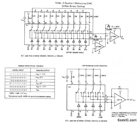
The following applications circuits are intended to illustrate the following points
.A 2-KΩ resistor should be in series with V+ to limit supply current with negative ringing of the bit inputs
.Temperature compensation for RDs(on) can be provided in the feedback path of the op amp
.Bipolar reference voltages can be used in all configurations (View)
View full Circuit Diagram | Comments | Reading(1126)
High_gain_video_amplifier
Published:2009/7/23 21:00:00 Author:Jessie
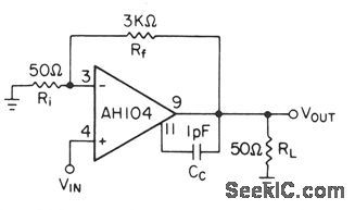
This circuit shows an AH104 used as a high-gain video amplifier. The high output-current capability makes the AH104 suitable for such high-frequency driver applications. In this circuit, a closed-loop gain of 60 can be obtained to 10MHz. For lower gains, Cc must be larger to promote stability. The power connections are the same as for Fig. 3-45. The AN103 can be used in this circuit, without Cc, but the internal 20-pF compensation capacitor reduces the gain at any given bandwidth. (View)
View full Circuit Diagram | Comments | Reading(672)
UJT_TRIAC_PHASE_CONTROL
Published:2009/7/23 21:00:00 Author:Jessie
Has wide range of stable control, without hysteresis or dependence upon supply voltage. Used in automatic feedback control systems, since ujt is essentially half of balanced bridge, with bulb-in unbalance detection.- Transistor Manual, Seventh Edition, General Electric Co., 1964, p 330. (View)
View full Circuit Diagram | Comments | Reading(1030)
Video_pulse_amplifier
Published:2009/7/23 20:59:00 Author:Jessie
This circuit shows a video pulse amplifier that uses the basic circuit of Fig. 3-44. Figure 3-45B shows a suggested PC layout. Notice that internal current-limiting resistors provide short-circuit protection to the common line, with a limit of 100-mA maximum. A short to either supply line can destroy the unit.Typical supply voltages are± 20 V. (View)
View full Circuit Diagram | Comments | Reading(745)
100_mA_CURRENT_REGULATOR
Published:2009/7/6 3:07:00 Author:May
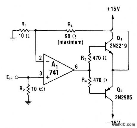
741 opamp is connected as noninverting voltage-controlled cuwent source feeding transistors that boost output and provide bidirectional current capability in load RL.If single-polarity currentflow is sufficient, omit opposite-polarity transistor.-W. G. Jung, IC Op-Amp Cookbook, Howard W. Sams, Indianapolis, IN, 1974, p 173. (View)
View full Circuit Diagram | Comments | Reading(5112)
| Pages:1052/2234 At 2010411042104310441045104610471048104910501051105210531054105510561057105810591060Under 20 |
Circuit Categories
power supply circuit
Amplifier Circuit
Basic Circuit
LED and Light Circuit
Sensor Circuit
Signal Processing
Electrical Equipment Circuit
Control Circuit
Remote Control Circuit
A/D-D/A Converter Circuit
Audio Circuit
Measuring and Test Circuit
Communication Circuit
Computer-Related Circuit
555 Circuit
Automotive Circuit
Repairing Circuit