
Circuit Diagram
Index 1057
20_MHz_video_log_amplifier
Published:2009/7/23 21:12:00 Author:Jessie
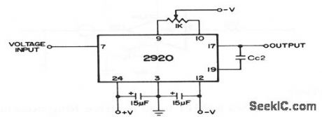
This circuit shows a 2920 in the basic log-amplifier configurations, using a minimum of external components. The offset pot between pins 9 and 10 is mandatory. Vcc is typically±15 V, C2 is typically between 10 and 50 pF. The circuit has a 20-MHz bandwidth and an 80-dB dynamic range. (View)
View full Circuit Diagram | Comments | Reading(744)
THREE_INPUT_TRIGGER
Published:2009/7/23 21:11:00 Author:Jessie
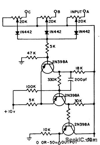
Digital logic permits use of only one Schmitt trigger for monitoring number of variables that can have different voltage levels at which trigger action is desired. Potentiometers provide independent control of set points for each positive input. Each input then triggers circuit independently at its particular theshold, pro vided circuit was not previously triggered. Circuit is taken from NASA-SP-5022 Technology Utilization Report, Lewis Research Center.-Multiple-Input Trigger Circuit, Electromechanical Design, Nov. 1965, p 66. (View)
View full Circuit Diagram | Comments | Reading(651)
PRECISION_THRESHOLD_DETECTOR
Published:2009/7/6 2:19:00 Author:May
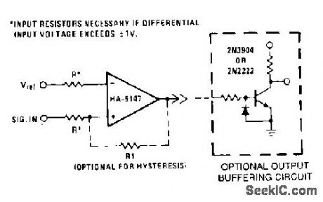
This circuit requires low noise, low and stable offset voltages, high open loop gain, and high speed. These requirements are met by the HA-5147. The standard variations of this circuit can easily be implemented using the HA-5147. For example, hysteresis can be generated by adding R1 to provide small amounts of positive feedback. The circuit becomes a pulse width modulator if Vref and the input signal are left to vary. Although the output drive capability of this device is excellent, the optional buffering circuit can be used to drive heavier loads, preventing loading effects on the amplifier. (View)
View full Circuit Diagram | Comments | Reading(1175)
LIGHTS_ON_REMINDER
Published:2009/7/6 2:19:00 Author:May
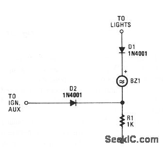
With both the ignition and the car lights on, piezo transducer BZ1 draws no current and remains silent. With only the ignition on, diode D1 is reverse-biased and so prevents current ftow through BZ1.
However, when the lights are on and the ignition is off, the transducer becomes energized and sounds to alert you to turn the lights off. With the ignition off and the lights on, D2 is reverse-biased, preventing current from flowing to the ignition.Resistor R1 prevents a short circuit when the ignitionison is on. (View)
View full Circuit Diagram | Comments | Reading(1357)
MULTIPLEXED_DISPLAY
Published:2009/7/6 2:19:00 Author:May
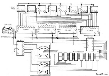
Used with battery-operated frequency Gaunter to reduce battery drain by multiplexing single decoder driver between all of MAN-4 displays, Readout is integrated by eye over total time period, making display appear continuous. Display operates at peak of 20 mA but duty cycle is only 12.5%.Counter is operated from 6-V supply. Four MC14021 8-bit shift registers implement multiplexing and provide latches needed to store count from MC14518 counter chain. Article describes operation in detail and gives circuit of companion front end and 5-MHz counter.-D.Aldridge, CMOS Counter Circuitry Slashes Battery Power Requirements, EDN Magazine, Oct. 20, 1974, p 65-71.
(View)
View full Circuit Diagram | Comments | Reading(1942)
PLL_BC_RECEIVER
Published:2009/7/6 2:18:00 Author:May
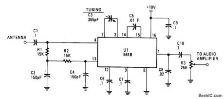
Circuit Notes
This simple AM circuit uses a 561B. There's no inductance/capacitance tuning circuit.The 365 pF capacitor connected between pins 2 and 3 does a11 the tuning. The circuit needs a good outside antenna and a solid ground. And if you want to further improve operation, stick a broadband amplifier in front of the receiver. Just make sure the input voltage does not climb over 0.5 volt rms. (View)
View full Circuit Diagram | Comments | Reading(1427)
EDGE_DETECTOR
Published:2009/7/6 2:16:00 Author:May
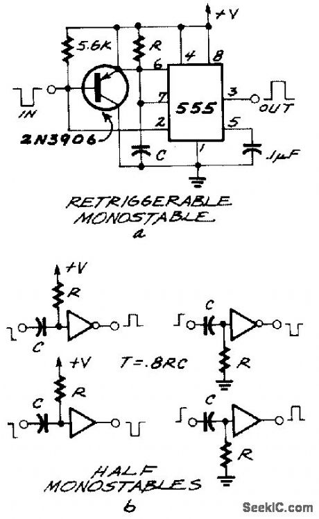
The 555 is a monostable that wants a negative-going trigger. If the pulse you're feeding it with is positive-going, you can run it through an inverter made up of either an inverting gate or, if you're tight on space, a single transistor. Both ways are shown. The circuits shown in Fig. 25-9b are edge detectors as well, and are usually referred to as half monostables, since they can't be used in every application. The width of the output pulse is deter-mined by the RC value, but there are a few rules governing their use:
.The input pulse has to be wider than the output pulse.The input pulse can't be glitchy. The circuit can't be retriggered faster than the RC time (View)
View full Circuit Diagram | Comments | Reading(0)
UPDATE_TO_100_MHz
Published:2009/7/6 2:16:00 Author:May
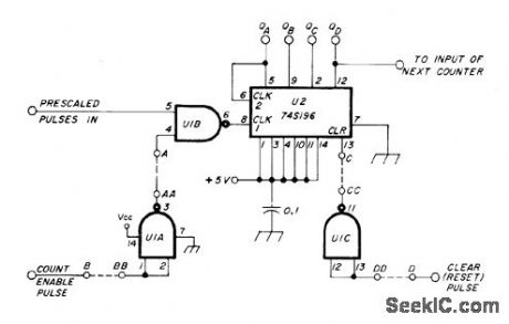
Simple counter stage can be added to input of existing frequency counter to extend direct counting range to 100 MHz, preparing it for use with 1-GHz prescaler.Use 74S196 presettable decade counter and 74S00 NAND-gate IC. If existing counter has positive reset pulse, connect C to CC and D to DD; if reset pulse is negative, connect C to D. If count enable pulse is negative, connect A to AA and B to BB; if positive, connect A to B. Power supply bypass capacitor should be shunted by 47-μF 10-V tantalum or electrolytic. Article covers modifications required in some counter input stages.-I. MacFarlane, How to Modify Your Frequency Counter for Direct Counting to 100 MHz, Ham Radio, Feb. 1978, p 26-29. (View)
View full Circuit Diagram | Comments | Reading(2104)
Microprocessor_supervisory_circuit_with_on_board_chip_enable
Published:2009/7/23 21:37:00 Author:Jessie
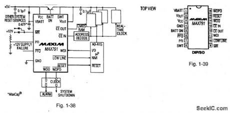
Figures 1-38 and 1-39 show a typical application circuit and pin configuration, respectively, for the MAX791. The IC is similar to that described for Figs. 1-J through 1-M, but with on-board chip-enable. The IC has a 200-ms reset pulse width, 1-μA standby current, 250-mA output in VCC mode, 25-mA output in battery-backup, 1.25-V threshold detector for power-fail warning, low-battery detection, or for monitoring a supply other than +5 V, a separate low-line comparator that compares VCC to a threshold 150 mV above the reset threshold, and a pulsed watchdog output to give advance warning of impending WDO assertion caused by watchdog timeout. MAX[M HIGH-RELIABILITY DATA Book, 1993, P. 5-35. (View)
View full Circuit Diagram | Comments | Reading(823)
12_bit_straight_binary_D_A_converter
Published:2009/7/23 21:37:00 Author:Jessie
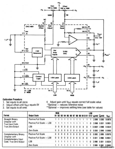
This circuit uses a DAC-4881 and a few external components to form a stand-alone, 0-to -10-V, D/A converter with both gain and offset adjustments for calibration. (View)
View full Circuit Diagram | Comments | Reading(564)
Low_cost_supervisory_circuit_with__3_V_monitoring
Published:2009/7/23 21:37:00 Author:Jessie
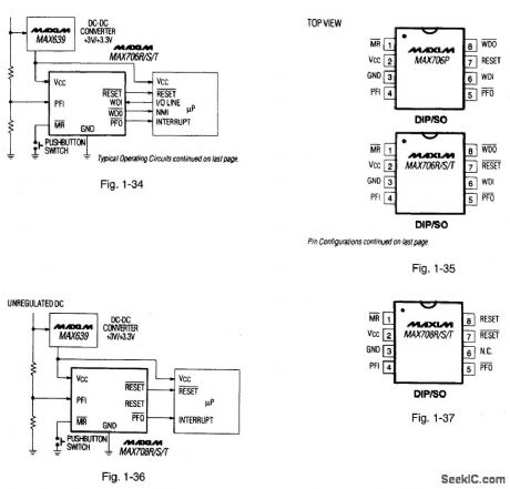
Figures 1-34 and 1-35 show a typical application circuit and pin configurations, respectively, for the MAX706P/R/S/T. Figures 1-36 and 1-37 show a typical application, circuit and pin configuration; respectively, for the MAX708R/S/T The ICs are similar to that described for Figs. 1-J through 1-M, but with the capability of monitoring +3-V supply levels. The ICs have a 200-ms reset pulse width, 100-pA quiescent current, a watchdog with 1.6-s timeout, and a 1.25-V threshold detector for power-fail warning, low-battery detection, or for monitoring supply levels in the +3-V to +5;V range. The difference among the MAX706R,S, and T is the reset-threshold levels, which are 2.63 V, 2.93 V and 3.08 V, respectively. All have active-low reset output signals. The MAX706P reset output is active-high with a 2.63-V threshold. The MAX708R/S/T are identical to the corresponding MAX706, except that the MAX708 series does not have a watchdog, but provides both RESET and RESET outputs. The watchdog is activated when the WDI input has not been toggled within 1,6 s. All of the ICs have an active-low manual reset.MAXIM HIGH-RELIABILITY DATA Book, 1993, P. 5-33, 5-34. (View)
View full Circuit Diagram | Comments | Reading(668)
Basic_current_to_voltage_converter
Published:2009/7/23 21:20:00 Author:Jessie
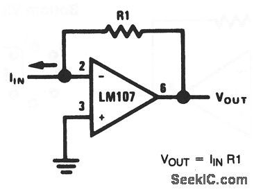
With this basic circuit, the input current is fed directly into the summing node (pin 2) and the op-amp output changes to extract the same current from the summing node through R1. The scale factor of this circuit is R1 volts per amp. That is, the output voltage is equal to the input current timesR1. The only conversion error in this circuit is Ibias, which is summed algebraically with IIN. The basic circuit can be used to measure current directly because: IIN =VOUT/R1. For example, if VOUT is 1 V (or 1000mV), and R1 is 100 Ω,IN = 10mA. (View)
View full Circuit Diagram | Comments | Reading(961)
BASE_TRIGGERING_WITH_HYBRID_GATE
Published:2009/7/23 21:18:00 Author:Jessie
Combines sensitivity of base triggering and trigger amplitude variation of collector triggering. Bias potential varies in order to direct trigger pulse more effectively. This steering scheme is attractive for some nonsaturated circuits, when collector-base voltage for conducting transistor is very small- Transistor Manual, Seventh Edition, General Electric Co., 1964, p 199. (View)
View full Circuit Diagram | Comments | Reading(758)
555 Narrow pluse Generator Circuit
Published:2011/7/30 3:09:00 Author:Zoey | Keyword: 555, Narrow pluse, Generator, Circuit
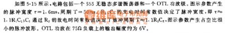
As shown in the figure 5-15, the circuit consists of a 555 astable multivibrator and an OTLPower Amplifier Stage. The parameter in the figure generates an pulse width r=1.6ms and a period T=50ms. The charge time constant determines the pulse width, that is , t≈1.1R1C1,and the pulse period T≈1.1R1C1 isdetermined by the charge time constant of R2. The parameter in the figure generates a pulse waveform that has a small duty cycle. When put on the 75 Ω load,the output magnitude of the amplifier OTLwill beabout 6V. (View)
View full Circuit Diagram | Comments | Reading(821)
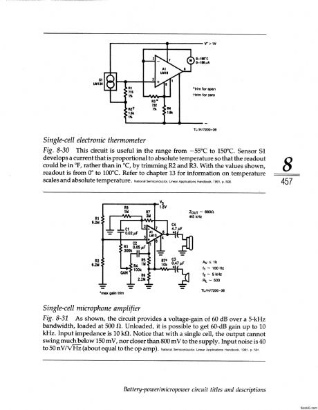
Ultra_low_noise_RIAA_preamp
Published:2009/7/23 21:18:00 Author:Jessie
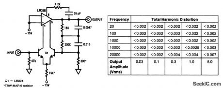
This circuit uses an LM394 and an LM318 to form an ultra-low noise preamp. Noise referred to a 10-mV input signal is -90 dB down, measuring 0.55μV and 70 pA in a 20-kHz bandwidth. The noise figure is less than 2 dB when the amplifier is used with standard phono cartridges, which have an equivalent wideband (20 kHz) noise of 0.7μV. Worst-case dc output offset voltage is about 1V with a 1-kΩ cartridge. THD for various output amplitudes is shown in the table. (View)
View full Circuit Diagram | Comments | Reading(3623)
Dc_coupled_tape_head_preamps_four_head
Published:2009/7/23 21:17:00 Author:Jessie
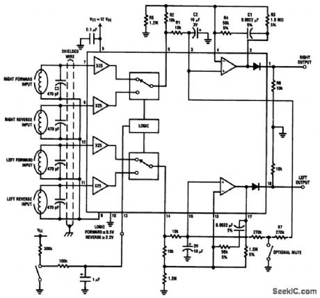
This circuit shows a dc-coupled, four-head stereo preamp using an LM1937. The desired pair of heads (for forward and reverse operation, where the heads are not mechanically repositioned) is controlled by the logic voltage at pin 13. The circuit characteristics are the same as for the circuit of Fig. 1-50. (View)
View full Circuit Diagram | Comments | Reading(856)
Resistor_multiplier
Published:2009/7/23 21:17:00 Author:Jessie
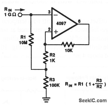
This circuit appears as a high resistance to the input. The resistance value depends on R1, R2, and R3 (1 GΩ using the values shown). (View)
View full Circuit Diagram | Comments | Reading(0)
1_MC_SCHMITT_TRIGGER
Published:2009/7/23 21:16:00 Author:Jessie
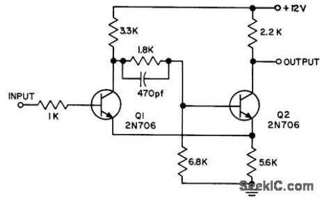
Q1 conducts when input exceeds 6.8 v. Q2 always conducts if input is below 5.2 v. Ambient temperature range is 0 to 71℃. Output at collector has 2 v minimum level change.- Transistor Manual, Seventh Edition, Geneml Electric Co., 1964, p 200. (View)
View full Circuit Diagram | Comments | Reading(801)
Typical_testing_troubleshooting_application_of_probe_and_pulser
Published:2009/7/23 21:16:00 Author:Jessie
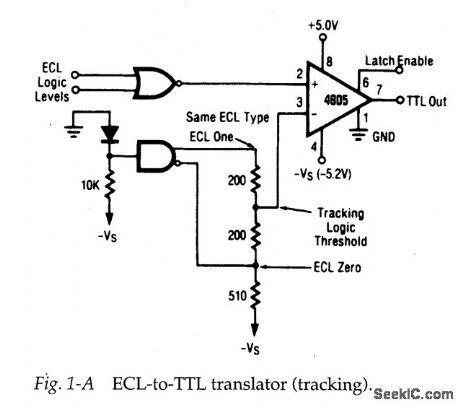
A circuit (such as Fig. 1-A) can be tested by applying a pulse at the input and monitoring the output. This can be done with a pulser (or signal generator) at the in-put and a probe (or scope) at the output. For example, pulses with ECL levels can be applied at the ECL-gate input and TTL pulses can be monitored at the output.If TTL pulses are absent at pin 7 of the 4805 comparator, check for pulses at pins 2 and 3. This procedure will isolate the problem to the gate or to the comparator. (View)
View full Circuit Diagram | Comments | Reading(636)
Fixed Period pulse 555 Generator with a changeable Duty cycle
Published:2011/7/30 3:09:00 Author:Zoey | Keyword: Fixed Period pulse, 555 Generator , changeable Duty cycle
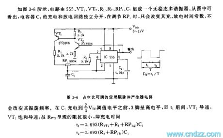

As shown in the figure 3-6,the astable multi-vibrator in the circuit consists of a 555 circuit, VT1,VT2, R1,R2,RP1 and C1.From the picture we can see that the capacitor C1 has a separate charge and discharge looped, the adjustment of RP1 will change its charge and discharge time constant instead of its oscillator frequency. Therefore, before C1 gets a 2/3 threshold level of VDD, pin 3willstayin high level, that is, during t1, VT2 will conduct, and VT1 will be saturated and conducted, thus, RVT1 presents a weak impedance, the charge time
t1=0.693(RVT1+R1+RP1left) C1
t2 =0.693(R2+RP1right) C1
T=t1+t2
=0.693((RVT1+R1+RP1) C1
DK=t1/T
then, adjust RP1 and the duty cycle can be limited in between 2%~98% with an unchanged period.
(View)
View full Circuit Diagram | Comments | Reading(1267)
| Pages:1057/2234 At 2010411042104310441045104610471048104910501051105210531054105510561057105810591060Under 20 |
Circuit Categories
power supply circuit
Amplifier Circuit
Basic Circuit
LED and Light Circuit
Sensor Circuit
Signal Processing
Electrical Equipment Circuit
Control Circuit
Remote Control Circuit
A/D-D/A Converter Circuit
Audio Circuit
Measuring and Test Circuit
Communication Circuit
Computer-Related Circuit
555 Circuit
Automotive Circuit
Repairing Circuit