
Circuit Diagram
Index 1046
TYPICAL_TWO_OP_AMP_BRIDGE_TYPE_DIFFERENTIAL_AMPLIFIER
Published:2009/7/6 4:44:00 Author:May
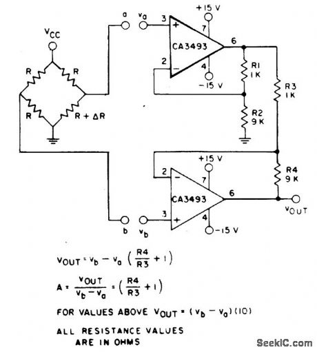
Using a CA3493 BiMOS op amp to provide high input impedance and good common-mode rejection ratio (depends primarily on matching of resistor networks). (View)
View full Circuit Diagram | Comments | Reading(586)
BRIDGE_CIRCUIT
Published:2009/7/6 4:43:00 Author:May
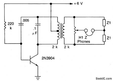
The transistor is connected as an audio oscillator, using an audio transformer in the collector. The secondary goes to a linear pot. The ratio between the two parts of the pot from the slider is proportional to the values of Z1 and Z2 when no signal is heard in the phones. (View)
View full Circuit Diagram | Comments | Reading(1782)
Video_distribution_amplifier_
Published:2009/7/23 20:22:00 Author:Jessie
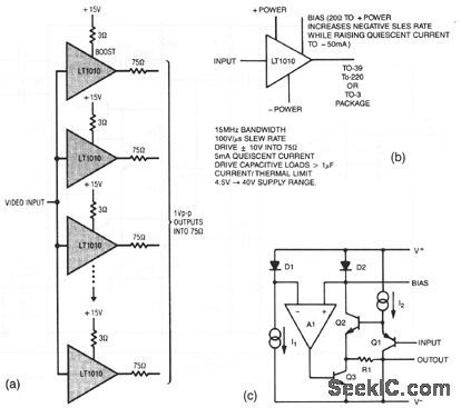
The resistors in the output lines are included to isolate reflections from unterminated lines. If the line characteristics are known, the resistors can be deleted. To meet NTSC gain-phase requirements, a small-value boost resistor is used. Figures 3-27B and 3-27C show the LT1010 characteristics. (View)
View full Circuit Diagram | Comments | Reading(1245)
BRIDGE_BALANCE_INDICATOR
Published:2009/7/6 4:42:00 Author:May
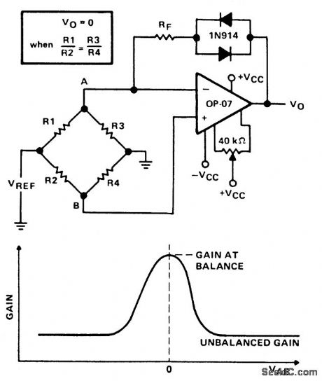
Indicator provides an accurate comparison of two voltages by indicating their degree of balance (or imbalance). Detecting small variations near the null point is difficult with the basic Wheatstone bridge alone. Amplification of voltage differences near the null point will improve circuit accuracy and ease of use.The 1N914 diodes in the feedback loop result in high sensitivity near the point of balance (R1/R2=R3/R4). When the bridge is unbalanced the amplifier's closed-loop gain is approximately RF/r, where r is the parallel equivalent of R1 and R3. The resulting gain equation is G = RF(1/R1+1/R3). During an unbalanced condition the voltage at point A is different from that at point B. This difference voltage (VAB), amplified by the gain factor G, appears as an output voltage, As the bridge approaches a balanced condition (R1/R2 = R3/R4), VAB approaches zero. As VAB approaches zero the 1N914 diodes in the feedback loop lose their forward bias and their resistance increases, causing the total feedback resistance to increase. This increases circuit gain and accuracy in detecting a balanced condition. The figure shows the effect of approaching balance on circuit gain. The visual indicator used at the output of the OP-07 could be a sensitive voltmeter or oscilloscope. (View)
View full Circuit Diagram | Comments | Reading(1373)
PORTABLE_NICAD_BATTERY_CHARGER
Published:2009/7/6 4:40:00 Author:May
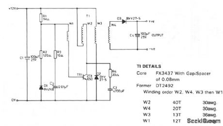
This circuit was designed to charge NiCad battery packs in the range of 4.8 to 15.6 V from a convenient remote power source, such as an automobile battery. When power is first applied to the circuit, a small bias current supplied by R1 via winding W1, starts to turn on the transistor TR1. This forces a volt-age across W2 and the positive feedback given by the coupling of W1 and W2 causes the transistor to turn hard on, applying the full supply across W2. The base drive voltage induced across W1 makes the junction between R1 and R2 become negative with respect to the 0-V supply, forward-biasing diode Dl to provide the necessary base current to hold TR1 on.
With the transistor on, a magnetizing current builds up in W2, which eventually saturates the ferrite core of transformer T1. This results in a sudden increase on the collector current flowing through TR1, causing its collector-emitter voltage to rise, and thus reducing the voltage across W2. The current flowing in W2 forces the collector voltage of the TR1 to swing positive until restricted by transformer output load-ing. Rc network R4 and C3 limits the turn off transient TR1. R3 and C2 maintain the loop gain of the circuit when diode D1 is not conducting.
(View)
View full Circuit Diagram | Comments | Reading(916)
FIBER_OPTIC_LINK
Published:2009/7/6 4:40:00 Author:May
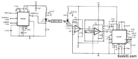
The circuit shows a simplex fiber link between the NE5080 transmitter and the NE5081 receiver. The components shown are for a center frequency of 5 MHz, although this frequency can be increased to 20 MHz with proper selection of external component values. The NE5539 has a 530-MHz unity gain bandwidth which could limit maximum operating frequencies in some systems. Since the NE5081 can adequately accept signals below 10 mV at 5-MHz carrier, the gain stage within the dashed lines can be eliminated if the attenuation in the link is low. If the gain stage is used, be mindful of the bandwidth tradeoff at higher gains. Refer to the NE5539 data sheet for details. (View)
View full Circuit Diagram | Comments | Reading(2609)
Video_line_driving_amplifier
Published:2009/7/23 20:20:00 Author:Jessie
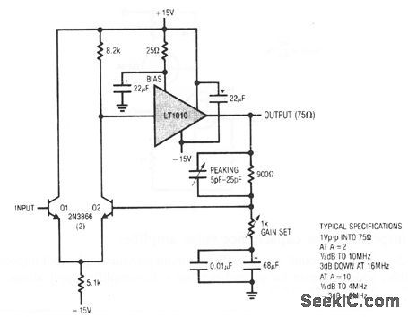
This circuit combines the LT1010's load-handling capability with a fast, discrete gain stage. Q1 and Q2 form a differential stage that single-ends into the LT1010. For video applications that are sensitive to NTSC requirements, dropping the bias resistor will aid performance. The peaking adjustment should be optimized under loaded output conditions. (View)
View full Circuit Diagram | Comments | Reading(0)
Minimum_component_bridge_amplifier
Published:2009/7/23 20:11:00 Author:Jessie
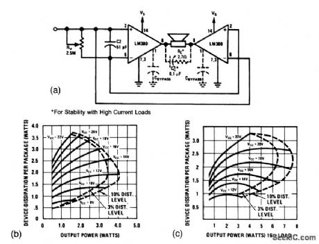
This circuit shows two LM380 ICs connected to double the audiooutput power of a single LM380.The Circuit provides twice the voltage swing across the load for a given supply, increasing the power capability by a factor of four over the single amplifier. However, in most cases, the package dissipation is the first parameter that limits power to the load. In such cases, the power capability of the bridge circuit is only twice that of the single IC. Figures 1-37B and 1-37C show output power versus device-package dissipation for both 8- and 16-Ω loads in the bridge configuration. Notice that the 3% and 10% harmonic distortion contours double back (because of the thermal limiting of the LM380). Different amounts of heatsinking will change the point at which the distortion contours bend. (View)
View full Circuit Diagram | Comments | Reading(795)
Dc_stabilized_1000_V_μs_op_amp
Published:2009/7/23 20:10:00 Author:Jessie
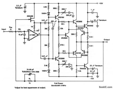
As shown,this circuit has a full power bandwidth to 8 MHz,with a slewrate of 1000-V/μs. (View)
View full Circuit Diagram | Comments | Reading(911)
AC_BRIDGE
Published:2009/7/6 4:38:00 Author:May
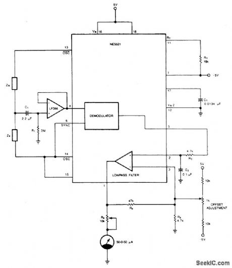
The circuit provides a simple and cost-effective solution to matching resistors and capacitors. Impedances ZR and Zx form a half-bridge, while OSC and OSC excite the bridge differentially. The external op amp is a FET input amplifier (LF356) with very low input bias current on the order of 30 pA (typical). C1 allows ac coupling by blocking the dc common mode voltage from the bridge, while RI biases the output of LF356 to 0 V at dc. Use of FET input op amp insures that dc offset due to bias current through R1 is negligible. Ac output of the demodulator is filtered via the uncommitted amp to provide dc voltage for the meter. The 10 k potentiometer, R5, limits the current into the meter to a safe level. Calibration begins by placing equal impedances at ZR and ZX, and the system offset is nulled by the offset adjust circuit so that Pin 1 is at 0 V. Next, known values are placed at Zx and the meter deviations are calibrated. The bridge is now ready to measure an unknown impedance at Zx with ±0.05% accuracy or better. (View)
View full Circuit Diagram | Comments | Reading(1085)
UJT_BATTERY_CHARGER
Published:2009/7/6 4:38:00 Author:May
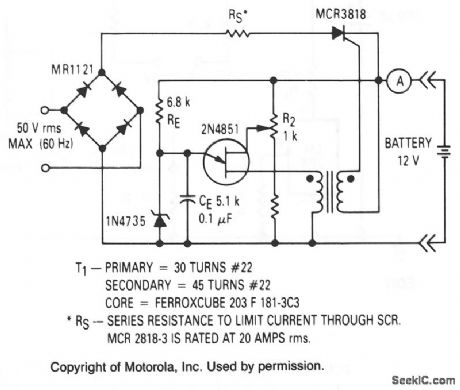
This circuit will not work unless the battery to be charged is connected with proper polarity. The battery voltage controls the charger and when the battery is fully charged, the charger will not supply current to the battery. The battery charging the current is obtained through the SCR when it is triggered into the conducting state by the UJT relaxation oscillator. The oscillator is only activated when the battery voltage is low.VB21 of the UJT is derived from the voltage of the battery to be charged, and since VP=VD=VB21; the higher VB21,the higher Vp. When Vp exceeds the breakdown voltage of the zener diode Z1, the UJT will cease to ftre and the SCR will not conduct. This indicates that the battery has attained its desired charge as set by R2. (View)
View full Circuit Diagram | Comments | Reading(1891)
TRANSFORMERLESS_BASE_MODULATOR
Published:2009/7/23 20:09:00 Author:Jessie
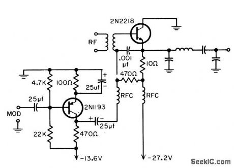
Requires only one audio transistor, and readily provides 100% modulation. Modulated output power is 660 mw for CB transmitter. Audio quality is excellent.-B. Rheinfelder, Modulation Techniques for Transistorized A.M Transmitters, FEE, 11:7, p 54-57. (View)
View full Circuit Diagram | Comments | Reading(1151)
50_Mb_s_FIBER_OPTIC_LED_DRIVER_
Published:2009/7/6 4:35:00 Author:May
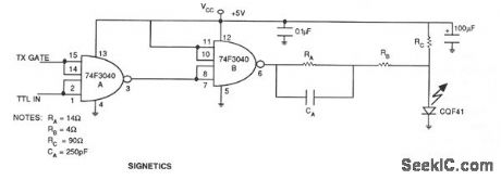
The pull-up transistor of the totem-pole output is used to turn on the LED and the pull-down transistor is used to turn off the LED. The lower impedance and higher current handling capability of the saturated pull-down transistor is used as an effective method of transferring the charge from the LED's anode to ground as its dynamic resistance increases during turn-off. The slightly higher output impedance of the pull-up stage ensures that the LED is not over peaked during the less difficult turn-on transition. This asymmetric current handling capability of the output stage with its variable impedance substantially reduces the pulse-width distortion and long-tai]ed response. As the signal propagates through two NAND gates, each transition passes through the high-to-low and low-to-high transition once, normalizing the total propagation delay through the circuit. (View)
View full Circuit Diagram | Comments | Reading(867)
Minimum_component_RIAA_phono_amp
Published:2009/7/23 20:07:00 Author:Jessie
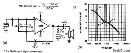
This circuit shows an LM380 used as a phono amplifier with RIAA playback characteristics. Figure 1-36B shows the playback response. (View)
View full Circuit Diagram | Comments | Reading(1047)
20_20000Hz_SINE_SQUARE
Published:2009/7/6 4:35:00 Author:May
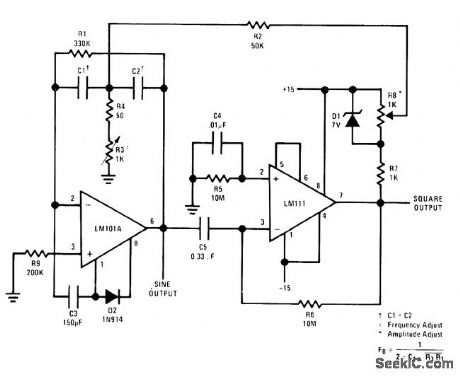
Opamp is used as tuned circuit driven by square wave from yoltage comparator Frequeny is controlled by R1-R3, C1, and C2, with R3 providing tuning.Comparator is fed with resulting sine wave to obtain square wave for feedback to input of tuned circuit, to cause oscillation. Zener stabifizes amplitude of square wave that is fed back.R6 and C5 provide DC negative feedback around comρarator to ensure starting.Values of C1 and C2 are equal,and range from 0.4 μF for 18-80Hz to 0.002 μF for 4.4-20 kHz.-''Easily Tuned Sine Wave Oscillator,″National Semiconducotor,Santa Clara,CA,1971,LB-16. (View)
View full Circuit Diagram | Comments | Reading(1074)
UNIVERSAL_BATTERY_CHARGER
Published:2009/7/6 4:34:00 Author:May
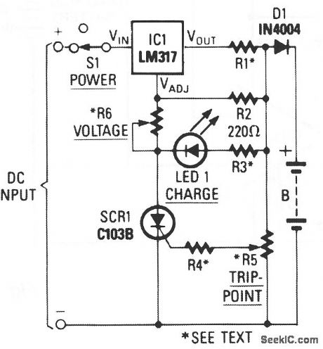
When power is applied to the circuit, SCR1 is off, so there is no bias-current path to ground; thus, LM317 acts as a current regulator. The LM317 is connected to the battery through steering diode D1, limiting resistor R1, and bias resistor R2. The steering diode prevents the battery from discharging through the LED and the SCR when power is removed from the circuit. As the battery charges, the voltage across trip-point potentiometer R5 rises, and at some point, turns on the SCR.Then, current from the regulator can flow to ground, so the regulator now functions in the voltage mode. When the SCR turns on, it also provides LED1 with a path to ground through R3. So, when LED1 is on, the circuit is in the voltage-regulating mode; when LED1 is off, the circuit is in the current-regulating mode. (View)
View full Circuit Diagram | Comments | Reading(5343)
LEAD_ACID_LOW_BATTERY_DETECTOR
Published:2009/7/6 4:32:00 Author:May
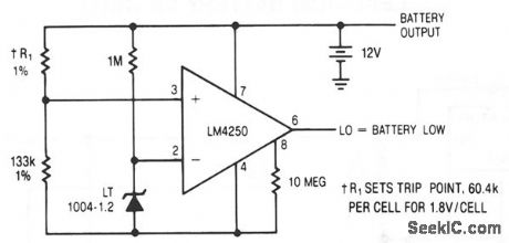
View full Circuit Diagram | Comments | Reading(776)
BATTERY_MONITOR
Published:2009/7/6 4:32:00 Author:May
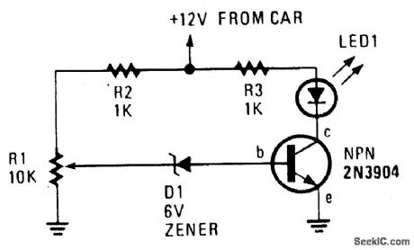
The circuit is quick and easy to put together and install, and tells you when battery voltage falls below the set limit as established by R1 (a 10,000-ohm potentiometer). It can indicate, via LED1, that the battery may be defective or in need of change if operating the starter causes the battery voltage to drop below the present limit. (View)
View full Circuit Diagram | Comments | Reading(0)
Linearized_platinum_resistance_thermometer
Published:2009/7/23 20:06:00 Author:Jessie
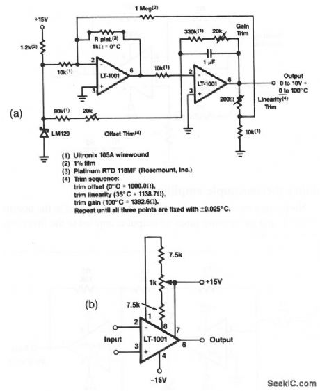
With the values shown, this circuit has a ±0.025°C accuracy over 0° to 100°C. The input offset voltage of the LT-1001, and its drift with temperature, are permanently trimmed at wafer test to a low level. However, if further adjustment of VOS is necessary, nulling with the circuit of Fig. 10-4B will not degrade drift with temperature. The Fig. 10-4B offset circuit has an approximate null range of ±100 μV. o Raytheon U near Integrated a rcuts 1989, p. 4-45. (View)
View full Circuit Diagram | Comments | Reading(715)
BATTERY_VOLTAGE_MONITOR
Published:2009/7/6 4:31:00 Author:May
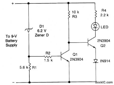
This circuit gives an early warning of the discharge of batteries. Zener diode D1 is chosen for the voltage below which an indication is required (9 V). Should the supply drop to below 7 V, D1 will cease conducting causing Q1 to shut off. Its collector voltage will now increase causing Q2 to start conducting via LED1 and its limiting resistor R4. (View)
View full Circuit Diagram | Comments | Reading(0)
| Pages:1046/2234 At 2010411042104310441045104610471048104910501051105210531054105510561057105810591060Under 20 |
Circuit Categories
power supply circuit
Amplifier Circuit
Basic Circuit
LED and Light Circuit
Sensor Circuit
Signal Processing
Electrical Equipment Circuit
Control Circuit
Remote Control Circuit
A/D-D/A Converter Circuit
Audio Circuit
Measuring and Test Circuit
Communication Circuit
Computer-Related Circuit
555 Circuit
Automotive Circuit
Repairing Circuit