
Circuit Diagram
Index 1051
3_TO_29_ODD_MODULO
Published:2009/7/6 3:19:00 Author:May
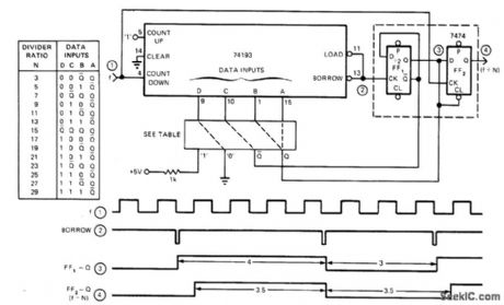
Basic dlvider using 74193 4-bit up/down counter and single 7474 dual D flip-flop provides any odd number of dlvider ratios from 3 to 29 by changing feedback connections as shown in table, all with symmetrical output waveforms. Based on writing any odd number N as N = M + (M + 1), where M is integer. Circuit forces counter to divide altemately by M and M + 1. Connection shown is for divide-by-7.-V. R. Godbole, Simplify Design of Fixed Odd-Modulo Dividers, EDN Magazine, June 5, 1975, p 77-78.
(View)
View full Circuit Diagram | Comments | Reading(2285)
10_Hz_TO_2_MHz
Published:2009/7/6 3:19:00 Author:May
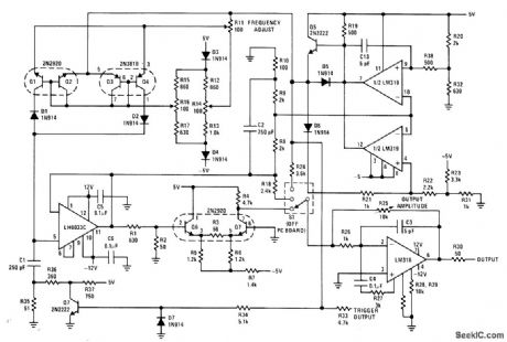
Triangle wave is generated by switching current-source transistors to charge and discharge timing capacitor. Precision dual comparator sets peak-to-peak amplitude. Sine converter requires close amplitude control to give low-distortion output from triangle input.Square-wave output is obtained at emitter of Q5, for driving current switches Q1-Q4 and LM318 output amplifier. Scaling permits adjusting all three waveforms to ±10 V. Waveforms are symmetrical up to 1 MHz, and output is usable to about 2 MHz.-R. C. Dobkin, Wide Range Function Generator, National Semiconductor, Santa Clara, CA, 1974, AN-115. (View)
View full Circuit Diagram | Comments | Reading(0)
Single_op_amp_difference_amplifier
Published:2009/7/23 20:39:00 Author:Jessie
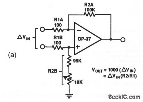
This circuit provides a voltage gain of 1000 for difference-signal inputs. For example, if the inverting input is 10 μV and the noninverting input is 11 μV, the difference is 1 μV and the output is 1000 μV. Figure 10-14B shows an offset nulling circuit (if required). (View)
View full Circuit Diagram | Comments | Reading(831)
DIVIDE_BY_15
Published:2009/7/6 3:17:00 Author:May
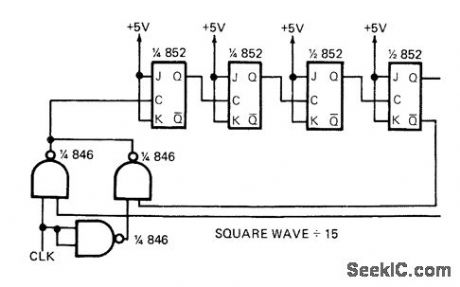
Input clock is altemately inverted and noninverted by gates operating in coniunction with 4 bits of storage using 852 JK flip-flops, to give square-wave output at 1/15 of clock frequency.-C. W. Hardy, Reader Responds to Odd Modulo Divider in July 1st EDN, EDN Magazine, Oct, 1, 1972, p 50. (View)
View full Circuit Diagram | Comments | Reading(713)
Parallel_data_acquisition_with_sample_hold
Published:2009/7/23 20:38:00 Author:Jessie
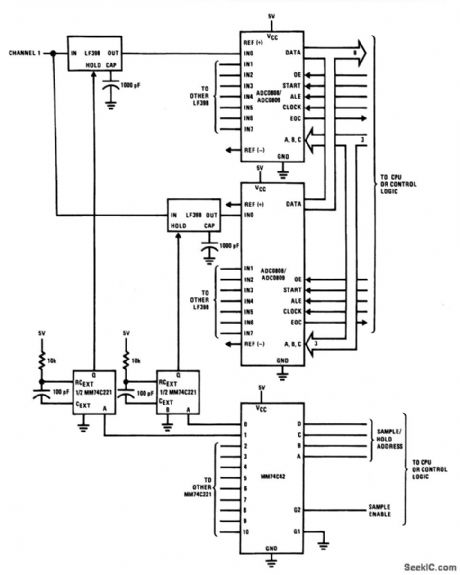
This circuit uses ADC0808/0809 ICs and LF398 sample/hold ICs to form an 8-channel parallel data-acquisition system. Sample/hold is accessed through an MM74C42 which pulses an MM74C221, generating a sample pulse. After each sample/hold has sampled the signal, the appropriate channel information is processed by the ADC (as described in Fig.6-13). (View)
View full Circuit Diagram | Comments | Reading(1780)
RELAY_DRIVER_PROVIDES_DELAΥ_AND_CONTROLS_CLOSURE_TIME
Published:2009/7/6 3:17:00 Author:May
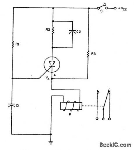
Circuit NotesThe relay operates a certain time, td, after power is applied to it, and then it operatesfor a leng付1 of time, tCThe SCR fires when the voltage on C1 reaches VA.This operatesthe relay, which stays activated until the current charging C2 drops below the dropoutcurrent. 10 keep the relay In its activated position indefinitely(tc=∞), ellmlnate C2and choose R2 just large enough to keep the relay coil current within its related limits, Typical component values for td=30 seconds and tc=2 seconds are∶ R1=1.5megohms, R2 = 10 k ohms, R3 =3 k ohms, C1=47μF, and C2 =100μF. TheSCR is a 2N1877 and the relay is a Potter Brumfield PW-5374. A value of 12 Vdc ISassumed for Vcc. (View)
View full Circuit Diagram | Comments | Reading(746)
UHF_PRESCALER
Published:2009/7/6 3:15:00 Author:May
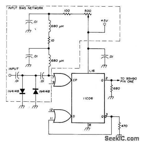
Uses Fairchild 11C06 700-MHz D flip-flop as divide-by-20 UHF prescaler with toggle rates in excess of 550 MHz from 0 to 75°C. Amplifier may be used in place of input bias network shown. Developed for use with 95H9O decade divider. Unused CP and D inputs are tied to ground.-D. Schmieskors, 1200-MHz Frequency Sealers, Ham Radio, Feb. 1975, p 38-40. (View)
View full Circuit Diagram | Comments | Reading(1000)
Analog_video_switch_and_amplifier_with_direct_coupled_output
Published:2009/7/23 20:38:00 Author:Jessie
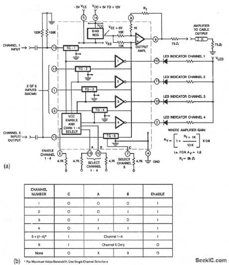
This circuit shows a CA3256 switch/amplifier connected for a direct-coupled output. One of four channels can be selected in parallel with channel 5. The analog switches of channels 1 to 4 are digitally controlled by logic (Fig. 3-35B). A VEE of -5 V is required. Vcc can be from +5 to +12 V. Amplifier gain is determined by the external resistor Rf, as shown by the equaeion. (View)
View full Circuit Diagram | Comments | Reading(809)
Mini_power_amplifier
Published:2009/7/23 20:37:00 Author:Jessie
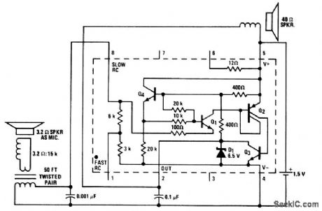
This little LM3909 audio amplifier can be operated as a one-way intercom or for listening in on various situations. Operating current is only 12 to 15 mA. The circuit can hear fairly faint sounds, and someone speaking directly into the microphone generates a full 1.4-V peak-to-peak at the speaker. (View)
View full Circuit Diagram | Comments | Reading(796)
Single_chip_TV_chroma_luma_processor
Published:2009/7/23 20:36:00 Author:Jessie
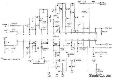
The CA3217E contains all required circuit functions between the video detector and picture-tube RGB driver stages of a color television receiver. The CA3217E decodes the chroma signals and then produces three different color signals that are internally combined with the luma to develop the RGB signals. The picture saturation, hue, and brightness controls are externally adjustable by the viewers. The AFPC, ACC, dynamic flesh control, beam limiting, and gate black-level (brightness) controls are servo loops that are used to stabilize the RGB output and reduce frequent manual adjustment. The automatic beam-limiter circuit reduces picture contrast and brightness to prevent excessive drive output at the picture tube. (View)
View full Circuit Diagram | Comments | Reading(1540)
DOOR_AJAR_MONITOR
Published:2009/7/6 3:15:00 Author:May
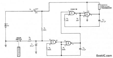
The monitor senses an ajar door and, if the situation isn't corrected within 20 seconds, sounds a beeping alarm. The circuit is controlled by a magnetic reed switch and magnet on the door. With the door closed, the switch is closed and the alarm is disarmed. Opening the door opens switch, C1 starts charging up through R1. Approximately 20 seconds later, the voltage at pin 9 is high enough to turn on the oscillator formed from C, D, R2, R3, and C2. That pulses the piezoelectric transducer's 3-kHz oscillator. For lower standby drain on the battery, change RI to 66 MO and C1 to 1 mF (film). (View)
View full Circuit Diagram | Comments | Reading(1856)
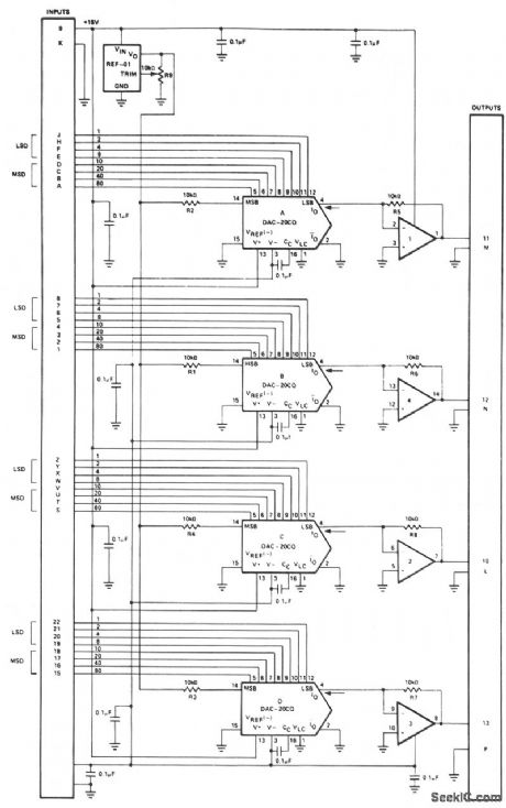
FOUR_CHANNEL_D_A_OUTPUT_AMPLIFIER
Published:2009/7/6 3:14:00 Author:May
View full Circuit Diagram | Comments | Reading(588)
AUTOMOBILE_AIR_CONDITIONER_SMART_CLUTCH
Published:2009/7/6 3:12:00 Author:May
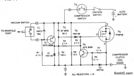
This circuit disables the air conditioner compressor when additional engine power is required. It does so by monitoring the engine vacuum at the intake manifold. If the vacuum drops to 40% of its normal level, the compressor clutch is disabled, removing the air conditioner load from the engine. After the engine returns to normal vacuum level, there is a 6 second delay before the compressor clutch is enabled and the air conditioner is reactivated. This allows 6 seconds of extra power, about 500 ft at 60 MPH, which increases the safety margin when passing another vehicle. Loss of cooling is minimal because the air conditioner fan is not interrupted. When the engine is accelerated, manifold vacuum drops and vacuum switch VS opens to 40% of the normal manifold pressure. This causes Q1 to turn on, discharging C2 and tuming off Q3 via diode D2. When Q3 tums off, so does Q2. When the engine reaches its normal operating vacuum, VS closes and Q1 turns off, allowing C2 to charge for 6 seconds until Q3 turns on again.
(View)
View full Circuit Diagram | Comments | Reading(566)
Noninverting_amplifier_for_gains_less_than_10
Published:2009/7/23 21:07:00 Author:Jessie
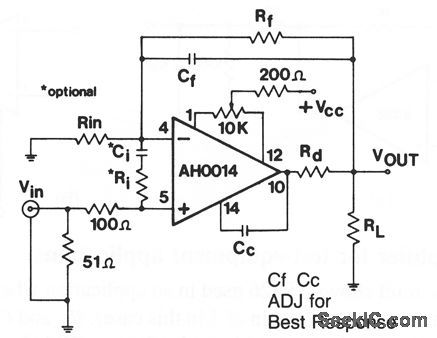
This circuit shows an AH0014 connected as a noninverting wideband amplifier, where gains must be less than 10, but more than 1. The characteristics are the same as for the circuits of Figs. 3-49 and 3-51. Figure 3-48B shows external connections for the AH0014. (View)
View full Circuit Diagram | Comments | Reading(649)
Mitsubishi Pajero light off-road vehicle assistant socket wiring circuit diagram
Published:2011/5/10 1:06:00 Author:Rebekka | Keyword: Mitsubishi Pajero, assistant socket
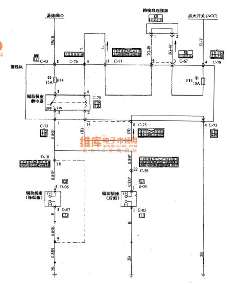
Mitsubishi Pajero light off-road vehicle assistant socket wiring circuit diagram is shown as above.
Wiring Color
B: Black LG: light green G: Green L: Blue W: White Y: Yellow SB: sky blue BR: Brown 0: Orange GR: Gray R: red P: Pink V: Purple (View)
View full Circuit Diagram | Comments | Reading(961)
PLL_DIVIDER
Published:2009/7/6 3:11:00 Author:May
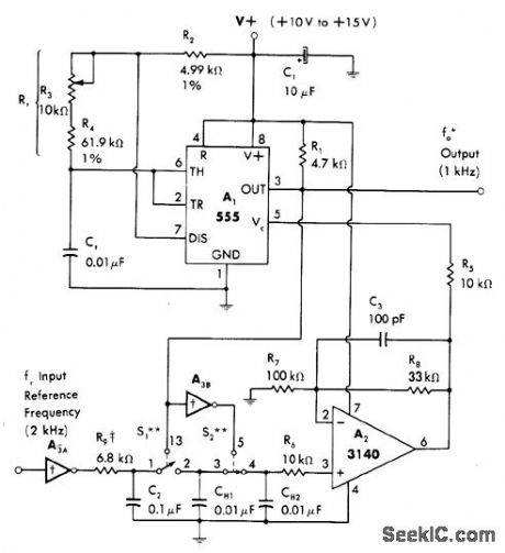
Simple phase-locked loop is suitable for generating integral submultiples M of input frequency. Values shown give M of 2.Square-wave input reference is limited in amplitude to supply voltage by first CMOS inverter A3A. RC network R9-C2, integrates output to give 2 V P-P triangle across C2 for sampling by sample-and-hold switch sections S1 and S2 of 4016 CMOS analog switch. Sampled error voltage of loop, stored on CH2, is read out by FET amplifier A2. Amplified error voltage is applied to A1 through R5 to induce changes in center frequency of A1 as required to maintain locked condition.-W. G. Jung, IC Timer Cookbook, Howard W. Sams, Indianapolis, IN, 1977, p 220-224.
(View)
View full Circuit Diagram | Comments | Reading(1019)
CONVENTIONAL_SCHMITT_TRIGGER
Published:2009/7/23 21:07:00 Author:Jessie
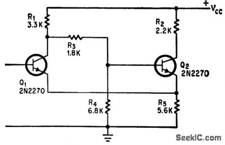
Q1 is turned on when input exceeds 6.5 v, and input remains clomped at this level. As a result, input signal cannot drive additional Schmitt circuits that may have higher trigger levels.-J. Gaon, Diode and Resistor Increase Input Resistance of Schmitt, Electronics, 39:12, p 110-111. (View)
View full Circuit Diagram | Comments | Reading(798)
_15_V_WITH_FEEDBACK
Published:2009/7/6 3:10:00 Author:May
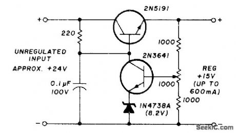
Fraction of output voltage is fed back to base of 2N3641 regulator transistor. Difference between this voltage and zener diode voltage is amplified to control base of 2N5191 series transistor.-H. Olson, Powet-Supply Servicing, Ham Radio, Nov. 1976, p 44-50. (View)
View full Circuit Diagram | Comments | Reading(1200)
Inverting_amplifier_for_gains_less_than_10
Published:2009/7/23 21:06:00 Author:Jessie

This circuit shows an AH0014 connected as an inverting wideband amplifier, where gain must be less than 10, but more than 1. The characteristics are the same as for the circuit of Fig. 3-49, but layout is more critical. Keep all leads as short as possible. Solder chip capacitors (bypass capacitors) directly to the chip pins. Use a ground plane. For best results, use an Ri of 1 kΩ or less, and keep Ci in the 15- to 60-pF range (use a variable Ci and adjust for best results. Figure 3-48B shows external connections for the AH0014. (View)
View full Circuit Diagram | Comments | Reading(664)
DIGITAL_TACH_DWELL_METER
Published:2009/7/6 3:10:00 Author:May
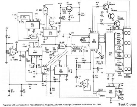
The heart of the circuit is IC2, a 4046 micropower phase-locked loop (PLL). The incoming signals are fed to the PLL after being buffered by IC1a and its associated components. The frequency of the incoming signal is multiplied by either 90, 60, or 45, depending on the setting of the cylinder select switch, S2. That switch selects the proper output from counters IC3 and IC4, which are set to divide the output frequency of the PLL by those amounts, and then send the divided output back to the comparator to the PLL to keep it locked on to the input signal. The phase pulses output at pin 4 of IC2, then go through an AND gate IC5d-which only passes the signals if the PLL is locked on to an input signal, preventing stray readings-and then to the input of IC6. When in the tach mode, IC6 counts the number of pulses present at pin 12, during the timing interval generated by IC8 and the associated circuitry of IClb. Because of the varied multiplication rate for the different cylinder selections-90, 60, and 45 for 4, 6, and 8 cylinders, respectively, the time interval is always constant at 1/3 of a second. The time interval is adjusted with R9, a 500-KΩ potentiometer; it is the only adjustment in the circuit.
In the high-tach (TACH 1 or x 100) range of 0- 9990 rpm, the output of IC2 is routed by switches S1a and S3 through IC7, a divide-by-ten counter, which increases the count range tenfold. In the low-tach (TACH 2 or x 10) range of 0- 999 rpm, the counter is bypassed.
(View)
View full Circuit Diagram | Comments | Reading(2108)
| Pages:1051/2234 At 2010411042104310441045104610471048104910501051105210531054105510561057105810591060Under 20 |
Circuit Categories
power supply circuit
Amplifier Circuit
Basic Circuit
LED and Light Circuit
Sensor Circuit
Signal Processing
Electrical Equipment Circuit
Control Circuit
Remote Control Circuit
A/D-D/A Converter Circuit
Audio Circuit
Measuring and Test Circuit
Communication Circuit
Computer-Related Circuit
555 Circuit
Automotive Circuit
Repairing Circuit