
Circuit Diagram
Index 1054
001_Hz_TO_100_kHz
Published:2009/7/6 2:53:00 Author:May
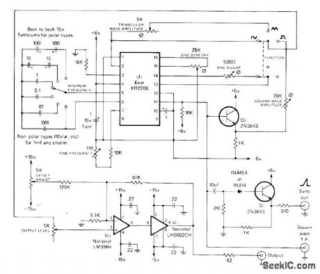
Variable DC offset permits adjustment of average value of sine, square, or triangle waveform to any arbitrary plus or minus value within voltage swing capability of opamp U3 Buffer stage U2 is inside feedback loop. Simple emitter-follower differentiator provides positive-going 1-V 0.5-μs output at sink terminal. Square-wave output is buffered by emitter-follower Q2.-H.Olson, The Function Generator, CQ, July 1975, p 26-28 and 71-72. (View)
View full Circuit Diagram | Comments | Reading(1085)
NULL_DETECTOR
Published:2009/7/6 2:52:00 Author:May
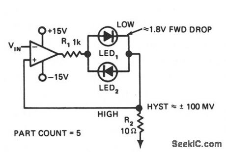
In this indicating comparator circuit, R2 setsthe hysteresis,If the 741 saturates at ±12 V. the current in R1 will be approximately±10 mA if 0.1 V hysteresis iS desired,Then 0.1 V/10 mA=10Ω=R2. (View)
View full Circuit Diagram | Comments | Reading(3163)
Mitsubishi Pajero light off-road vehicle front and rear window wiper washing wiring circuit diagram
Published:2011/5/10 0:59:00 Author:Rebekka | Keyword: Mitsubishi Pajero, light off-road vehicle , front and rear window
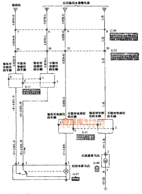
Mitsubishi Pajero lightoff-road vehicle before and after the window wiper washing wiring circuit diagram is shown as above. (View)
View full Circuit Diagram | Comments | Reading(732)
Mitsubishi Pajero light off-road vehicle before and after window wiper washing circuit diagram
Published:2011/5/10 0:58:00 Author:Rebekka | Keyword: Mitsubishi Pajero
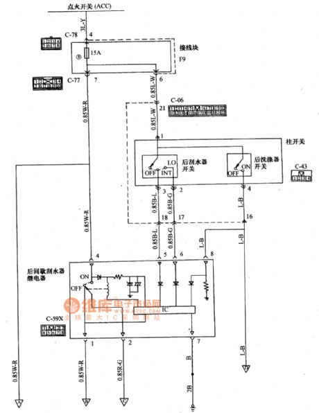
Mitsubishi Pajero light off-road vehicle before and after window wiper washing circuit diagram is shown as above. (View)
View full Circuit Diagram | Comments | Reading(1196)
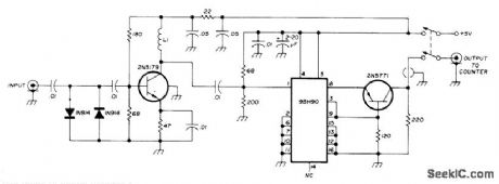
LOW-DRAIN_2_MHz_FRONT_END
Published:2009/7/6 2:49:00 Author:May
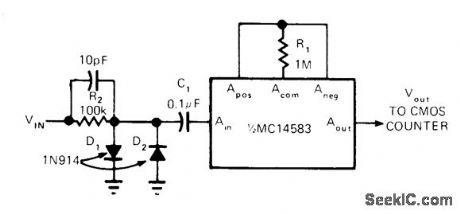
Simple CMOS linear front end for 5-MHz battery-operated counterreduces power drain and makes it proportional to input frequency,With no input,drain is only a few microamperes Half of COUNTER MC14583 CMOS Schmitt trigger forms front end operating from single 6-V battery used In counter,Upper frequency limit is about 3 MHz,and input sensitivity is 400 mV.-D Aldridge,CMOS Counter Circuitry,Slashes Battery Power Requirements,EDN Magazine,Oct,20,1974,p 65-71.
(View)
View full Circuit Diagram | Comments | Reading(1058)
WAVEFORM_GENERATOR
Published:2009/7/6 2:48:00 Author:May
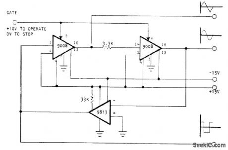
Two Optical Electronics 9008 integrators and 9813 comparator together generate choice of sine, square, and triangle waveforms suitable for system testing and display generation. Square wave is typically± 13.5 V with 20-μs transition time. Trianglewave is ±10V with better than 0.1% triangle linearity. Comparator senses zero crossings of sine-wave output to produce square waves, thus completing feedback loop. Integrators are commanded at pin 8 for zero output, so triangle and sine outputs can be made to start from zero.-''Waveform Generator, Optical Electronics, Tucson, AZ, Application Tip 10257. (View)
View full Circuit Diagram | Comments | Reading(0)
HIGH_BANDWIDTH_PEAK_DETECTOR
Published:2009/7/6 2:48:00 Author:May
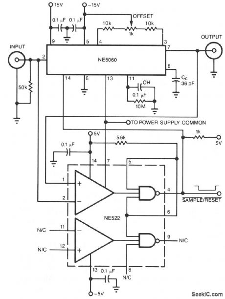
The high-speed peak detector uses a highly accurate, fast s/h amplifter controlled by a highspeed comparator. The s/h amplifter holds the peak voltage, until the comparator switches the amp to its sample mode, to capture a new, higher voltage level. The circuit handles all common-wave shapes and exhibits 5% accuracy from 50 Hz to 2 MHz.
The comparator's output decreases when the input signal exceeds the value of the currently held output. This transition puts the s/h amplifter into sample mode. Once the output reaches the value of the input, or the input signal falls below the output's level, the comparator's output increases; the high output brings the s/h amplifter back to the hold mode, thereby holding the peak value of the input signal. Reset the circuit by lowering the value of pin 4 of the NE522 comparator, which in turn allows the NE5060 s/h amplifter to acquire the input. The NE522 comparator has an open-collector output. (View)
View full Circuit Diagram | Comments | Reading(1341)
THREE_TIME_BASE_WlNDOWS
Published:2009/7/6 2:48:00 Author:May
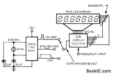
Intersil 7207A crystal-controlled timer generates precision gate windows of10 ms,100 ms, and 1 s for use as time bases, calibration markers, or gate timerns for frequency counters such as 7208.-B.O'Neil, IC Timers-the Old Reliable 555 Has Company, EDN Magazine, Sept. 5, 1977, p 89-93.
(View)
View full Circuit Diagram | Comments | Reading(887)
300_MHz_PRESCALER_1
Published:2009/7/6 2:46:00 Author:May
Divides inputfrequency by 10 for extending range of digital frequency counter up to prescaler limit of 300 MHz. Reading of counter must be multiplied by 10. Article also gives circuits of high-resolution counters using CMOS TTL devices.-H. E. Harris, Simplifying the Digital Frequency Counter,Raido,Feb 1978,p 22-25. (View)
View full Circuit Diagram | Comments | Reading(4027)
MAGNETIC_TAPE_FLAW_DETECTOR
Published:2009/7/23 21:52:00 Author:Jessie
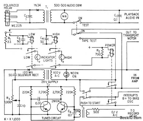
Transistor oscillator records steady test lone on tape. Machine stops during playback when repro-duced level indicates law that would make tape unsuitable for broadcast use. Polarized relay charges memory capacitor as it responds to transient. Capacitor discharges into coil of slower relay, which in turn slops transport. -N. J. Thompson, Detector Pin-Points Magnetic Tape Flaws, Electronics, 32:2, p 50-51. (View)
View full Circuit Diagram | Comments | Reading(1032)
TRANSISTORIZED_UHF_TV_TUNER
Published:2009/7/23 21:52:00 Author:Jessie
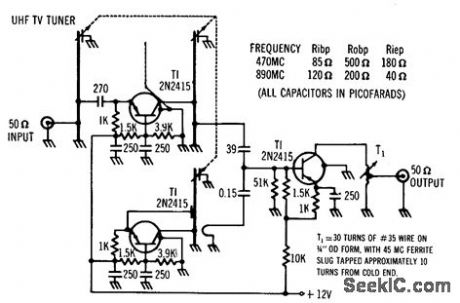
Gain is 3 to 9 db over tuning range of 470 to 890 Mc and noise-figure is 7 to 9 db, with output at 45 Mc. Current drain is only 18 ma at 12 v.-Transistorized UHF Tuner Features Low Noise, High Gain, Electronics, 36:2, p 15. (View)
View full Circuit Diagram | Comments | Reading(3023)
Differentiator
Published:2009/7/23 21:52:00 Author:Jessie
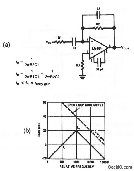
This circuit was originally developed to perform the mathematical operation of differentiation in analog computers. As shown by the frequency-response plot of Fig. 10-40B, a differentiator is actually a form of filter. R2/C2 form a 6-dB per octave rolloff network in the feedback, and R1/C1 form a similar network at the input. (View)
View full Circuit Diagram | Comments | Reading(1553)
100_MHz_CRYSTAL_OSCILLATOR
Published:2009/7/6 2:44:00 Author:May
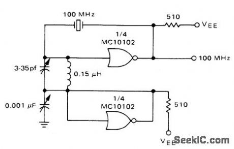
Developed for frequency counter that uses standard ECL components. Crystal can be changed to 10 MHz when measuring TTL performance.-W. B.Blood, Jr., Measure Frequency and Propagation Delay whh High Speed MECL Circuits, Motorola, Phoenix, AZ, 1972, AN-586 p 3.
(View)
View full Circuit Diagram | Comments | Reading(89)
Bipolar_offset_true_zero_D_A_converter
Published:2009/7/23 21:48:00 Author:Jessie
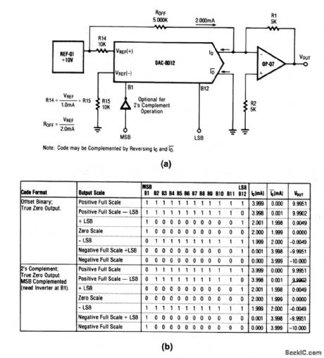
This circuit shows a DAC/op-amp combination that is bipolar-offset (true zero) operation. Full-scale adjustment can be in Fig. 6-39B. (View)
View full Circuit Diagram | Comments | Reading(642)
DIGITAL_PEAK_DETECTOR
Published:2009/7/6 2:44:00 Author:May
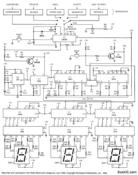
The peak detector tracks and holds, using the charge-storing ability of a capacitor, the highest output voltage from a transducer. Initially, the voltage on the inverting input of the comparator is at ground level. As a small voltage (0- 5 V) is captured by the peak detector and presented to the comparator's noninverting input, the output will swing high, which assets the bilateral switch; clock pulses now pass through the switch to clock both the BCD and binary counters. The outputs of the binary counters are connected to an R2R ladder network, which functions as a digital-to-analog converter. As the binary count increases, the R2R ladder voltage also increases until it reaches a point slightly above the voltage of the peak detector; at that instant, the comparator output swings low, which disables the bilateral switch and stops the counters.The number displayed on the 7-segment LED's vgill represent a value equivalent to the transducer's output. (View)
View full Circuit Diagram | Comments | Reading(1496)
Miniature_AM_radio_receivers
Published:2009/7/23 21:48:00 Author:Jessie
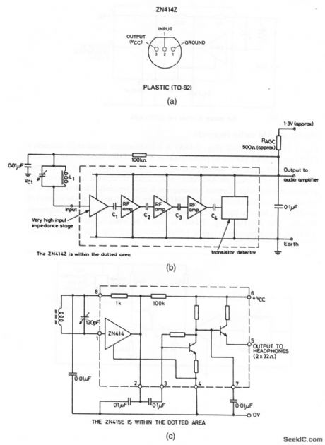
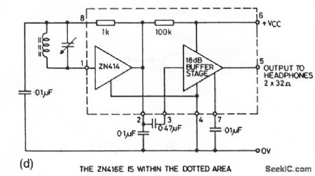
The ZN414Z (Fig. 2-14A) is a 10-transistor tuned-radio-frequency (TRF) circuit in a 3-pin TO-92 plastic package (Fig. 2-14B). The ZN414Z provides a complete RF amplifier, detector and AGC circuit that requires only six external components to produce an AM tuner. AGC action is adjusted by selecting one external resistor value. Current consumption is low (typically 2 to 4 mA), and no set-up or alignment is required. The ZN415E (Fig. 2-14C) retains all the features of the ZN414Z, but also includes a buffer stage that is capable of driving headphones directly. The ZN416E (Fig. 2-14D) is also a buffered-output version of the ZN414Z, which provides a typical 120 mV (rms)output into a 64-Ω load. (View)
View full Circuit Diagram | Comments | Reading(1555)
PREAMP_FOR_CMOS_LOGIC
Published:2009/7/6 2:44:00 Author:May
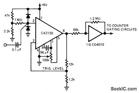
Combination of CA3130 and CD4010 ICs provides broad fre-quency response at very low power levels, as required for driving frequency counter. Diodes protect input from overvoltage. Amplifier offset control pot is used as trigger level control. Input sensitivity of amplifier/trigger combination is 50 mV P-P from 1 Hz to 1 MHz.-R. Tenny, Counter Pre-Amp Matches CMOS Logic Capability, EDN Magazine, Sept. 20, 1976, p 114 and 116. (View)
View full Circuit Diagram | Comments | Reading(1645)
BASIC_SQUAREN_TRIANGLE
Published:2009/7/6 2:43:00 Author:May
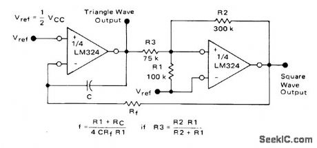
Requires only two sections of LM324 quad differential-input opamp to provide choice of triangle or squarewave outputs at frequency determined by values of components. Supply voltage range is 3-32 V.- Quad Low Power Operational Amplifiers, Motorola, Phoenix,AZ, 1978, DS 9339 R1.
(View)
View full Circuit Diagram | Comments | Reading(2776)
10_Hz_TO_2_MHz
Published:2009/7/6 2:41:00 Author:May
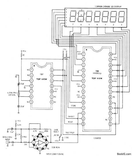
Seven-decade Intersil 7208 latched and multiplexed frequency counter with direct digit and display drive obtains timing waveform from 7207 IC which dlvides6,5536-MHz crystal oscillator output by 212 to produce 1600-Hz square, ave for multiplexing counter and display. Square wave is further divided to produce 0.1-sand 0.01-s counting gates along with reset and update commands. RCA 3130 opamp is used for conditioning of input signaL-D. Lancaster, CMOS Cookbook, Howard W. Sams, Indianapolis, IN, 1977, p 380-382.
(View)
View full Circuit Diagram | Comments | Reading(2656)
10_1_SCALER
Published:2009/7/6 2:40:00 Author:May
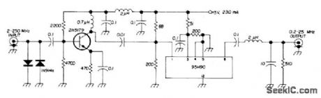
Used to increase range of frequency counter. Sensitivity is 20 mV at 175 MHz, 40 mV at 220 MHz, and 90 mV at 250 MHz.Fairchild IC is used. Simple L-section filter at output rolls off frequencies above 30 MHz, allowing sealer to be used up to 250 MHz without erroneous counting of second or third harmonics of squarewave output of scaler if counter in use will respond to 60 MHz or more.-E. Guerri, Frequency Pre-Scaler, Ham Radio, Feb. 1973, p 57. (View)
View full Circuit Diagram | Comments | Reading(1621)
| Pages:1054/2234 At 2010411042104310441045104610471048104910501051105210531054105510561057105810591060Under 20 |
Circuit Categories
power supply circuit
Amplifier Circuit
Basic Circuit
LED and Light Circuit
Sensor Circuit
Signal Processing
Electrical Equipment Circuit
Control Circuit
Remote Control Circuit
A/D-D/A Converter Circuit
Audio Circuit
Measuring and Test Circuit
Communication Circuit
Computer-Related Circuit
555 Circuit
Automotive Circuit
Repairing Circuit