
Circuit Diagram
Index 1047
Minimum_component_phono_amp_with_common_mode_volume_and_tone_controls
Published:2009/7/23 20:06:00 Author:Jessie
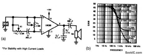
This circuit has a distinct advantage over the circuit of Fig. 1 -33. When transducers of high source-impedance are used, the full input impedance of the amplifier is realized. The circuit also has an advantage with transducers of low source impedance because the signal attenuation of the input voltage divider is eliminated.Figure 1 -35B shows the tone-control response. (View)
View full Circuit Diagram | Comments | Reading(974)
FIBER_OPTIC_TRANSMITTER
Published:2009/7/6 4:30:00 Author:May
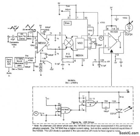
This receiver circuit consists of wideband differential amplifier NE592, VCO NE564 and LED driver NE522-the high-speed comparator. The video signal is ac coupled into the modulator preamplifier and followed by a sync tip clamp to provide dc restoration on the composite video signal and to prevent variation of modulation deviation with varying picture content. A video signal level of 250 to 300 mV peak is required to maintain optimum picture modulation. Frequency compensation (preemphasis) is inserted in the form of a passive rc lead network at the input to the NE592 differential amplifier. The main FM modulator consists of an NE564 used only as a linear wideband VCO, but the other sections of the device are not used. Differential dc coupling to the VCO terminals is attained via the loop filter terminals, pins 4 and 5. (View)
View full Circuit Diagram | Comments | Reading(3966)
PUT_BATTERY_CHARGER
Published:2009/7/6 4:25:00 Author:May
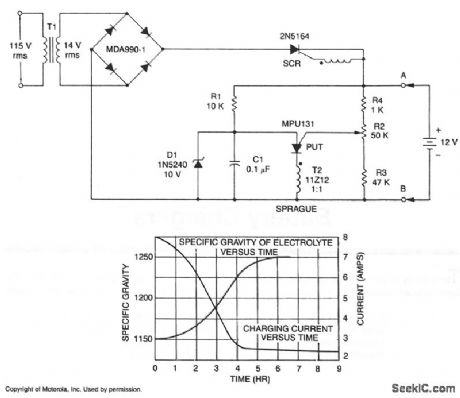
A short-circuit-proof battery charger will provide an average charging current of about 8 A to a 12-V lead/acid storage battery. The charger circuit has an additional advantage; it will not function nor will it be damaged by improperly connecting the battery to the circuit. With 115 V at the input, the circuit commences to function when the battery is properly attached. The battery provides the current to charge the timing capacitor C1 used in the PUT relaxation oscillator. When C1 charges to the peak point voltage of the PUT, the PUT fires turning the SCR on,which in turn applies charging current to the battery. As the battery charges, the battery voltage increases slightly which increases the peak point voltage of the PUT.This means that C1 has to charge to a slightly higher voltage to fire the PUT. The voltage on C1 increases until the zener voltage of Dl is reached, which clamps the voltage on C1, and thus prevents the PUT oscillator from oscillating and charging ceases. The maximum battery voltage is set by potentiometer R2 which sets the peak point firing voltage of the PUT. In the circuit shown, the charging voltage can be set from 10 V to 14 V-the lower limit being set by Dl and the upper limit by T1. (View)
View full Circuit Diagram | Comments | Reading(939)
TOTEM-POLE_DRIVER_WITH_BOOTSTRAPPING
Published:2009/7/6 4:23:00 Author:May

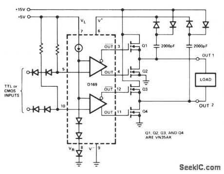
When driving MOSPOWER in a totem-pole output conftguration, it is necessary to have the gate voltage 10 to 15 V positive with respect to the source in order to handle load currents near the MOSPOWER maximum ratings. The D169 lends itself to bootstrapping because of its high-voltage ratings. In the circuit shown, the voltage on the 2000-pF bootstrap capacitors is applied via diode OR gates to the V+ terminal. Therefore, regardless of which output is high, 30 V is present at V +.Maximum switching frequency is determined by the input capacitance of the MOSPOWER transistors used. (View)
View full Circuit Diagram | Comments | Reading(1847)
BASIC_PNPN_MEMORY
Published:2009/7/23 2:10:00 Author:Jessie
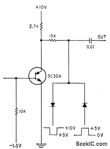
Delivers either positive or negative pulse output, accomplished by means of coupling diodes and transition memory capacitor.-J. B. Hangstefer and L. H. Dixon, Jr., Triggered Bistable Semiconductor Circuits, Electronics, 32:35, p 58-60. (View)
View full Circuit Diagram | Comments | Reading(667)
125_WATT_150_MHz_AMPLIFIER
Published:2009/7/6 4:22:00 Author:May
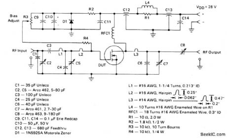
Circuit Notes
This amplifier operates from a 28 Vdc supply. It has a typical gain of 12 dB, and can survive operation into a 30:1 VSWR load at any phase angle with no damage. The amplifier has an AGO range in excess of 20 dB. This means that with input power held constant at the level that provides 125 watts output, the output power may be reduced to less than 1.0 watt continuously by driving the dc gate voltage negative from its IDQ value. (View)
View full Circuit Diagram | Comments | Reading(730)
AF_SINE_SQUARE_TRIANGLE
Published:2009/7/6 4:21:00 Author:May
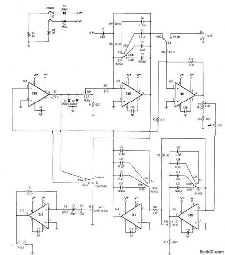
Can be tuned over entire audio spectrum in four ranges for generation of low-distortion waves for laboratory use. IC1 converts sine wave to square wave. IC3 acts as integrator converting squarewave output of IC1 to triangle wave. IC4-IC6 form statevariable filter for removing sinewave componentfrom triangle wave. IC2 is simple inverting amplifier for output.-R.Melenand H. Garland,″Understanding lC Operational Amplifiers,″Howard W.Sams,Indianapolis,IN,2nd Ed.,1978,p 130-134.
(View)
View full Circuit Diagram | Comments | Reading(1053)
6_METER_PREAMPLIFIER_PROVIDES_20_dB_GAIN_AND_LOW_NF
Published:2009/7/6 4:19:00 Author:May
Circuit NotesC1, C2, and C3 are miniature ceramic or plastic trimmers. T1 (main winding) is 0.34μH. Use of 11 turns of no. 24 enameled wire on a T37-10 toroid core. The antenna winding has one turn, and Q1 the source winding has three turns. T2 primary consists of 11 turns of no. 24 enameled wire on a T37-10 toroid. Tap Q1 drain is three turns from C2 the end of the winding. The secondary has three turns. T3 is the same as T2, except its secondary has one turn. (View)
View full Circuit Diagram | Comments | Reading(710)
DIODE_MODIFIED_SCHMITT_TRIGGER
Published:2009/7/23 2:08:00 Author:Jessie
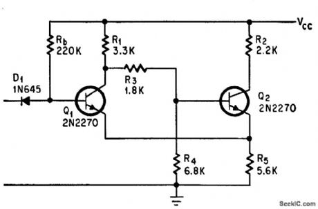
Addition of Rb and D1 reduces loading on driving circuit when Q1 is on, there by preventing input signal from being clamped. Same signal may therefore drive other Schmitt triggers having higher trigger levels.-J. Gaon, Diode and Resistor Increase Input Resistance of Schmitt, Electronics, 39:12, p 110-111. (View)
View full Circuit Diagram | Comments | Reading(879)
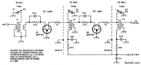
5_W_RF_POWER_AMPLIFIER
Published:2009/7/6 4:13:00 Author:May
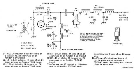
Circuit NotesNumbered components are so designated for PC-board layout purposes. C5 and C8 are disc ceramic. C6 and C7 are tantalum or electrolytic. R1, R2 and R3 are 1/2W carbon composition resistors. Silver-mica capacitors may be substituted for polystyrene (P) types. Impedance transformation ratios are shown above T1 and T2. (View)
View full Circuit Diagram | Comments | Reading(966)
Simple_Z80_interface_for_A_D_converter
Published:2009/7/23 2:04:00 Author:Jessie
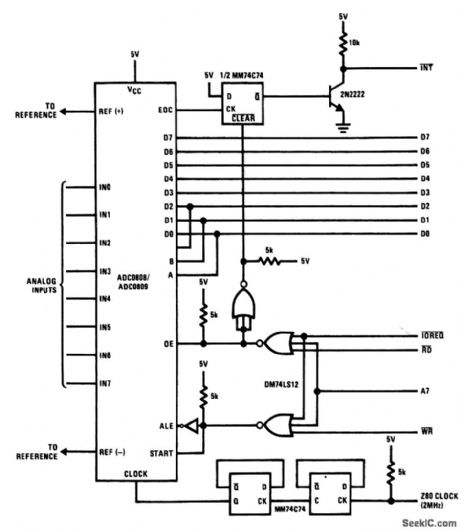
This circuit shows a simple Z80 interface for the ADC0808/0809, The inter-face is similar to that of Fig. 6-20, except that the interrupt is flip-flop closer to the 6800 (because of the Z80 INT is active low as in the 6800, but the INS8080 is active high). (View)
View full Circuit Diagram | Comments | Reading(509)
SQUARE_TRIANGLE_AF
Published:2009/7/6 4:13:00 Author:May
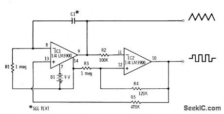
Two sections of LM3900 quad opamp are connected to generate dua-polarity triangle-and square-wave AF outputs while oρerating from single supply, byusing current mirror circuit at noninverting input Value used for C1 determines frequency and pulse width;frequency ranges from 0.5 Hz with 1 μF to 3800 Hz with 0.0001 μF and 21 kHzwith C1 omitted, Pulse-width rangeis 35μs without C1 to 1.6 s with 1 μF.-F.M Mims,″Integrated Circuit Projects,Vol.5,″Radio Shack,Fort Worth,TX,1977、2nd Ed. p 57-63 (View)
View full Circuit Diagram | Comments | Reading(831)
1_WATT,23_GHz_AMPLIFIER
Published:2009/7/6 4:07:00 Author:May

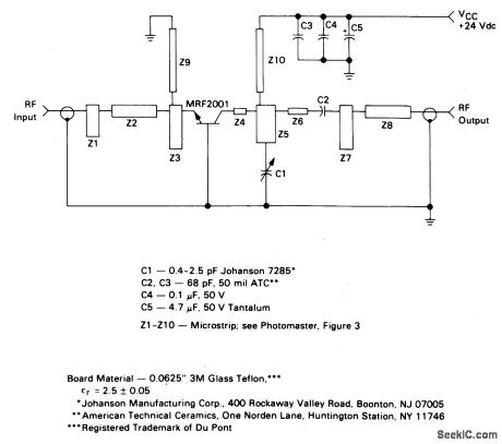
Circuit Notes
Simplicity and repeatability are feature-d in this 1 watt S-band amplifier design. The design uses an MRF2001 transistor as a common base, Class C amplifier. The amplifier delivers 1 watt output with 8 dB minimum gain at 24 V, and is tunable from 2.25 to 2.35 GHz. Applications include microwave communications equipment and other systems requiring medium power, narrow band amplification. The amplifier circuitry consists almost entirely of distributed microstrip elements. A total of six additional components, including the MRF2001, are required to build a working amplifier. The input and output impedances of the transistor are matched to 50 ohms by double section low pass networks. The networks are designed to provide about 3% 1 dB power bandwidth while maintaining a collector efficiency of approximately 30%. There is one tuning adjustment in the amplifier-C1 in the output network. Ceramic chip capacitors, C2 and C3, are used for dc blocking and power supply decoupling. Additional low frequency decoupling is provided by capacitors C4 and C5. (View)
View full Circuit Diagram | Comments | Reading(741)
Minimum_component_phono_amp_with_common_mode_volume_control
Published:2009/7/23 1:36:00 Author:Jessie
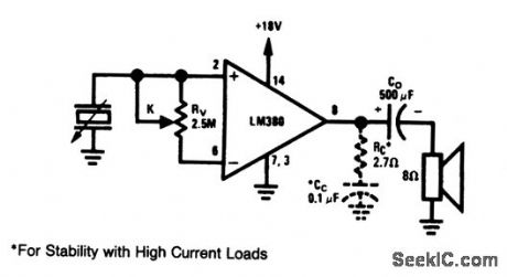
This circuit shows an LM380 as a phono amplifier with common-mode volume control.When in the full-volume position, the only source-loading impedance is the IC input impedance. This reduces to one-half the amplifier input impedance at the zero-volume position. (View)
View full Circuit Diagram | Comments | Reading(967)
LOW_POWER_RS_232C_DRIVER
Published:2009/7/6 4:05:00 Author:May
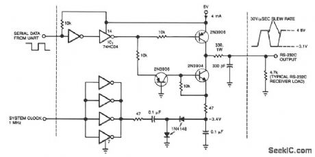
This circuit draws only 4 mA from a 5-V supply while driving a standard RS-232C receiver. The system clock drives a dc-dc converter that produces -3.4 V. The frequency can range from 0.5 to 8 MHz, but a range of 0.5 to 1 MHz will minimize power dissipation. The circuit output withstands direct shorts to ground or to either of the supplies (±12 V max). In place of the 74HC04 high-speed CMOS driver shown, you may want to substitute miscellaneous spare gates; one noninverting buffer, for example, can replace the two inverting types that receive the UART signal. (View)
View full Circuit Diagram | Comments | Reading(620)
LINE_SYNCHRONIZED_DRIVER
Published:2009/7/6 3:59:00 Author:May
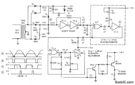
The gate drive that phase controls the four parallel SCRs is accomplished with complementary MOS hex gate MC14572 and two bipolar transistors. This adjustable line-synchronized driver permits SCR conduction from near zero to 180 degrees. A Schmitt trigger clocks a delay monostable multivibrator that is followed by a pulse-width monostable multivibrator. Line synchronization is achieved through the half-wave section of the secondary winding of the full-wave, center-tapped transformer. This winding also supplies power to the circuit through rectifiers D1 and D2. (View)
View full Circuit Diagram | Comments | Reading(2352)
SINE_COSINE
Published:2009/7/6 3:58:00 Author:May
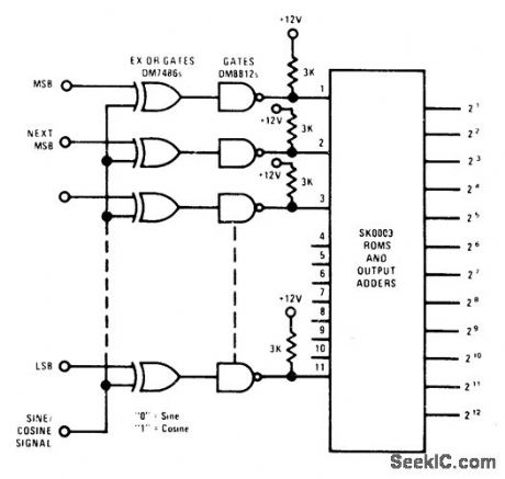
Uses National SK0003 sine/cosine look-up table kit consisting of four MOS ROMs and three output adders. Combination implements equation sin θ=sin M cos L + cos M sin L.Worst-case error is 1 5/8 bits in least significant bit. Cosine is approximated with loss in resolution of1/2 bit in 11-bit input or1/4 bit in 10-bit input.- Memory Databook, National Semiconductor, Santa Clara, CA, 1977, p 6-98-6-99. (View)
View full Circuit Diagram | Comments | Reading(991)
LOW_DISTORTION_16_TO_30_MHz_SSB_DRIVER
Published:2009/7/6 3:57:00 Author:May
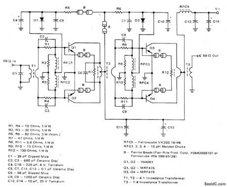
Circuit Notes
The amplifier provides a total power gain of about 25 dB, and the construction technique allows the use of inexpensive components throughout. The MRF476 is specified as a 3 watt device and the MRF475 has an output power of 12 watts. Both are extremely tolerant to overdrive and load mismatches, even under CW conditions. Typical IMD numbers are better than -35 dB, and the power gains are 18 dB and 12 dB, respectively, at 30 MHz. The bias currents of each stage are individually adjustable with R5 and R6. Capacitors C4 and CIO function as audio-frequency bypasses to further reduce the source impedance at the frequencies of modulation. Gain leveling across the band is achieved with simple RC networks in series with the bases, in conjunction with negative feedback. The amplitude of the out-of-phase voltages at the bases is inversely proportional to the frequency as a result of the series inductance in the feedback loop and the increasing input impedance of the transistor at low frequencies. Conversely, the negative feedback lowers the effective input impedance presented to the source (not the input impedance of the device itself) and with proper voltage slope would equalize it. With this technique, it is possible to, maintain an input VSWR of 1.5:1 or less than 1.6 to 30 MHz. (View)
View full Circuit Diagram | Comments | Reading(787)
Minimum_component_intercom
Published:2009/7/23 20:19:00 Author:Jessie

With switch S1 in the Talk position, the master-station speaker acts as the microphone. A T1 turns ratio of25 and an IC gain of 50 allows a maximum loop gain of 1250. RV provides a common-mode volume control. Switching S1 to Listen reverses the role of the master and remote speakers. Nationd Sem conductor Linear Appficatons Handbook 1991, p 200. (View)
View full Circuit Diagram | Comments | Reading(1118)
High_frequency_video_switch
Published:2009/7/23 20:19:00 Author:Jessie
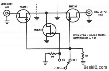
This circuit is similar to that of Fig. 3-22, except that this circuit is used when complete attenuation (rather than variable gain) is required in video applications. The 2N4391 provides a low on-resistance of 30Ωand a high off-impedance. With proper layout (separating input from output by the maximum allowable distance), and an ideal switch, the attenuation and insertion loss shown can be achieved with no difficulty. (View)
View full Circuit Diagram | Comments | Reading(911)
| Pages:1047/2234 At 2010411042104310441045104610471048104910501051105210531054105510561057105810591060Under 20 |
Circuit Categories
power supply circuit
Amplifier Circuit
Basic Circuit
LED and Light Circuit
Sensor Circuit
Signal Processing
Electrical Equipment Circuit
Control Circuit
Remote Control Circuit
A/D-D/A Converter Circuit
Audio Circuit
Measuring and Test Circuit
Communication Circuit
Computer-Related Circuit
555 Circuit
Automotive Circuit
Repairing Circuit