
Circuit Diagram
Index 2213
5V、5A Switching Regulators Power Circuit Diagram
Published:2011/3/21 1:44:00 Author:Rebrecca | Keyword: Switching Regulators

5V、5A Switching Regulators Power Circuit Diagram is shown as below.
(View)
View full Circuit Diagram | Comments | Reading(1465)
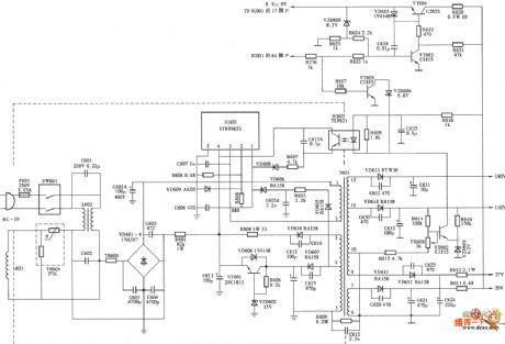
LCD TV power supply circuit diagram
Published:2011/3/27 20:34:00 Author:Rebekka | Keyword: LCD TV
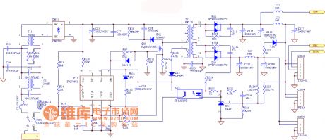
LCD TV power supply circuit diagram is shown as below.
(View)
View full Circuit Diagram | Comments | Reading(14064)
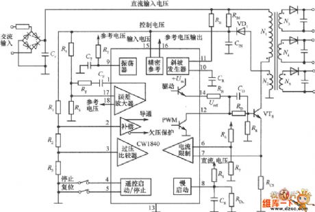
±15V Tracking Regulator Power Supply Circuit Diagram Six
Published:2011/3/21 1:44:00 Author:Rebrecca | Keyword: Tracking Regulator
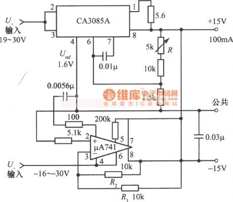
±15V Tracking Regulator Power Supply Circuit Diagram Six is shown as below.
(View)
View full Circuit Diagram | Comments | Reading(738)
Protect circuit diagram of filter capacitor in electronic rectifier
Published:2011/3/28 3:51:00 Author:Nicole | Keyword: filter capacitor, electronic rectifier
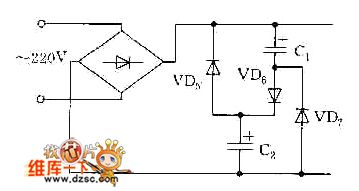
View full Circuit Diagram | Comments | Reading(513)
Switching tube drive circuit diagram composed of EXB 841
Published:2011/3/28 3:37:00 Author:Nicole | Keyword: switching tube drive
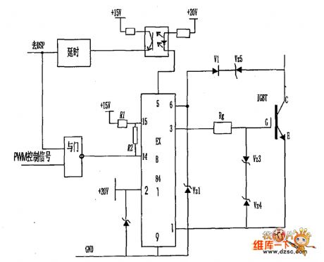
View full Circuit Diagram | Comments | Reading(488)
Shenyang sanyo AC double speed elevator main circuit
Published:2011/3/25 3:49:00 Author:Jessie | Keyword: AC, double speed elevator
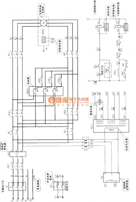
View full Circuit Diagram | Comments | Reading(751)
Single-ended flyback converter switching power supply circuit diagram
Published:2011/3/24 0:40:00 Author:Nicole | Keyword: converter, switching power supply
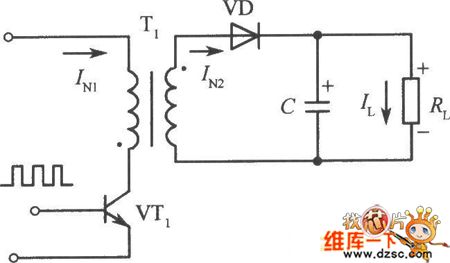
Single-ended flyback power converter switching power supply is not composed only by a transistor, the single-ended converter switching power supply also can be made of two transistors. The fundamental difference between Single-ended flyback switching power supply and the push-pull, full bridge, half-double-ended converter switching power supply is that the core of high-frequency transformer only work on one side of its hysteresis loop. The schematic of atypical single-ended flyback converter switching power supply as shown. The so-called single-ended, that means the core of converting circuit only work on one side of its hysteresis loop. The so-called flyback, that means when the transistor turns on, the energy stored in the primary induction coil, when the transistor is off, the energy stored in the primary coil will release to the load through the secondary coil. When the switching tube VT1 was motivated to turn on, the input voltage Ui will be applied to the primary winding N1 of high-frequency transformer T1. Due to the secondary rectifier diodes VD of transformer T1 was reversed, so there is no current flow on the secondary winding N2. When VT1 end, the voltage of winding N2 was polarity reversed, VD was positively skewed, the energy during VTl turns on stored in T1 will released through VD load.
(View)
View full Circuit Diagram | Comments | Reading(3730)
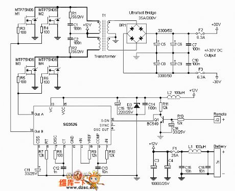
15V/3.5A 52W switching power supply circuit diagram composed of MC33374T/TV
Published:2011/3/23 22:32:00 Author:Nicole | Keyword: 52W switching power supply
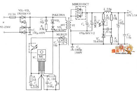
15V/3.5A 52W switching power supply circuit composed of MC33374T/TV as shown. The allowed range of AC input voltage is 92 ~ 276V. Rectifier bridge VD1 ~ VD4 use four 1N5406 3A/600V silicon rectifier tubes. Primary protection circuit is composed of RC absorber circuit (R2, C2) and the clamp circuit (VDz, VD5), it can effectively suppress the peak voltage due to the leakage of high-frequency transformer, to protect the internal power switch of MC33374 from damaged. VDz adopts P6KE200A transient voltage to suppress the diode(TVS), then the reverse breakdown voltage UB = 200V. VD5 uses MURl60 super fast recovery diode (SRD). Note, the serial number of RC R1, C3 in the figure is vacant, according to the need, it can turn the series circuit of R2, C2 into the R1 (20kΩ, 2W) and C3 (0.1μF, 400V) in parallel and then serial ultrafast recovery diode, formed R, C, VD protection circuit.
C5 is the bypass capacitor of Vcc side. S for control switching power supply, the key of on/of. After in series with R7 S, it can improve the reliability of mode conversion. VD6 and C6 form the high-frequency rectifier filter of the feedback coil output. Secondary high-frequency rectifier uses Schottky diode with high current, low voltage the model is MBR20100CT (20A/100V). The tube is common cathode, the two negative electrodes (cathode) are short circuited interiorly, it needs the two positive(anode) connected in parallel externally. C8, C11, L, C12 and C13 form the output filter circuit. In view of the inductance of filter inductance L is small, only 5.0μH, and large-capacity filter capacitors C8, Cl1 have equivalent inductance Lo, it will directly affect the actual inductance from L into L + Lo, so it should take the voice φ0.55mm enamelled wire with 7-turn around the feeder ring N3, and around the middle of the frame, to reduce leakage; also should around two layers of polyester film. The model of ferrite core is E25. In order to prevent saturated magnetization, it should stay out of the air gap of 0.43mm between the two E-shaped cores.
(View)
View full Circuit Diagram | Comments | Reading(4649)
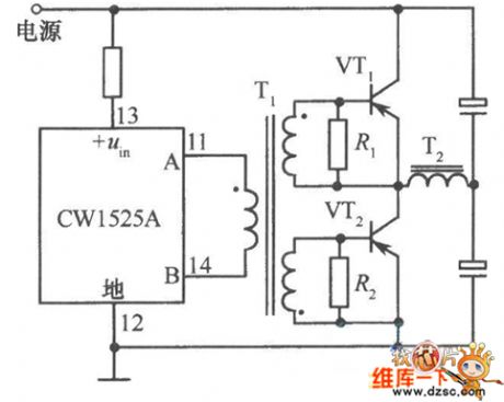
Push-pull circuit diagram with CWl525A driven diode
Published:2011/3/24 4:03:00 Author:Nicole | Keyword: driven diode
View full Circuit Diagram | Comments | Reading(661)
Low power switching power supply circuit diagram
Published:2011/3/22 2:25:00 Author:Nicole | Keyword: switching power supply
View full Circuit Diagram | Comments | Reading(808)
Skyworth 3T30 color TVs switching power supply circuit diagram
Published:2011/3/22 2:24:00 Author:Nicole | Keyword: Skyworth, switching power supply
View full Circuit Diagram | Comments | Reading(2043)
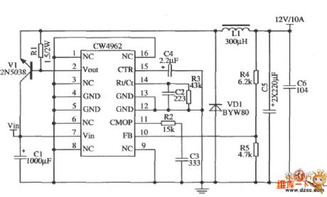
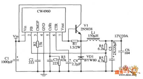
Extended output current circuit diagram with CW4962/CW4960
Published:2011/3/24 3:53:00 Author:Nicole | Keyword: output current
View full Circuit Diagram | Comments | Reading(797)
Multiple integrated switching regulator L4970A/L4975A/L4977A(L4972A/L4974A) circuit diagram
Published:2011/3/22 1:18:00 Author:Nicole | Keyword: integrated switching regulator
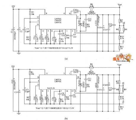
View full Circuit Diagram | Comments | Reading(3883)
5.1V regulator circuit diagram composed by L4970A、L4975A、L4977A
Published:2011/3/22 1:13:00 Author:Nicole | Keyword: 5.1V regulator
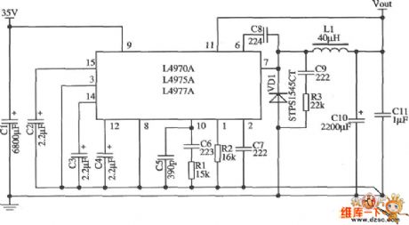
View full Circuit Diagram | Comments | Reading(3528)
5.1V/10A regulator circuit diagram composed of L4972A、L4974A
Published:2011/3/23 2:01:00 Author:Nicole | Keyword: 5.1V/10A regulator
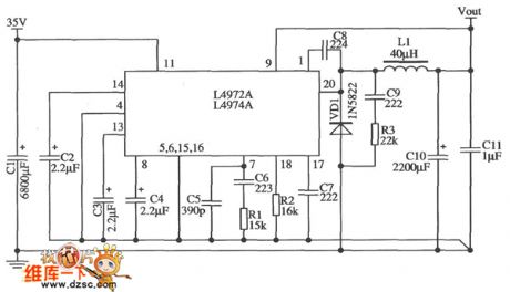
View full Circuit Diagram | Comments | Reading(2083)
MAX840/MAX843/MAX844 Integrated switching regulator circuit diagram
Published:2011/3/22 1:03:00 Author:Nicole | Keyword: Integrated switching regulator
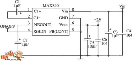
View full Circuit Diagram | Comments | Reading(744)
Application circuit diagram of reducing the voltage output resistance
Published:2011/3/24 3:18:00 Author:Nicole | Keyword: output resistance
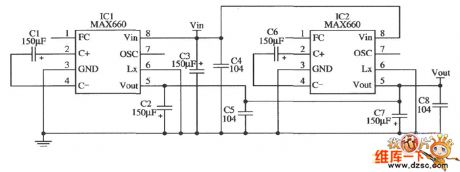
In order to reduce the output resistance (reduce voltage drop), it can parallel up to a few pieces of MAX660, as shown. Then its output resistance is the output resistance of Rout = MAX660 / n (n is the number of MAX660 chip).
(View)
View full Circuit Diagram | Comments | Reading(615)
Based on LM/LT Multifunction switch integrated regulator application circuit diagram
Published:2011/3/22 1:00:00 Author:Nicole | Keyword: Multifunction switch, integrated regulator

View full Circuit Diagram | Comments | Reading(1008)
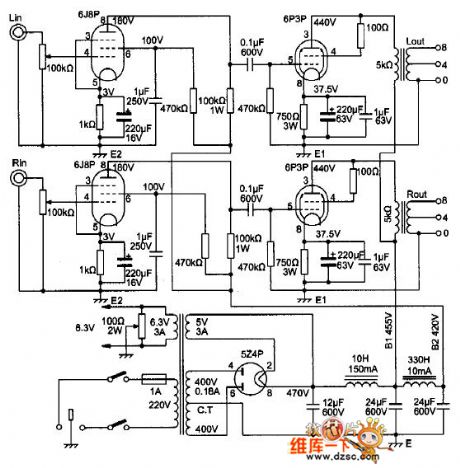
A class single-ended power amplifier circuit diagram with 6P3P triode Connection
Published:2011/3/25 1:27:00 Author:Nicole | Keyword: single-ended power amplifier, triode
View full Circuit Diagram | Comments | Reading(3416)
12V 30W---50W Subwoofer circuit diagram
Published:2011/3/24 19:51:00 Author:Nicole | Keyword: 30W---50W Subwoofer, 12V Subwoofer
View full Circuit Diagram | Comments | Reading(7692)
| Pages:2213/2234 At 2022012202220322042205220622072208220922102211221222132214221522162217221822192220Under 20 |
Circuit Categories
power supply circuit
Amplifier Circuit
Basic Circuit
LED and Light Circuit
Sensor Circuit
Signal Processing
Electrical Equipment Circuit
Control Circuit
Remote Control Circuit
A/D-D/A Converter Circuit
Audio Circuit
Measuring and Test Circuit
Communication Circuit
Computer-Related Circuit
555 Circuit
Automotive Circuit
Repairing Circuit