
Circuit Diagram
Index 2210
Logic input level remote-controlled integration fixed voltage power supply circuit diagram
Published:2011/3/22 22:05:00 Author:Rebekka | Keyword: Logic input , level remote-controlled integration , fixed voltage power supply
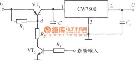
Logic input level remote-controlled integration fixed voltage power supply circuit diagram is shown as below.
(View)
View full Circuit Diagram | Comments | Reading(581)
555 touching timing switch circuit diagram
Published:2011/3/27 21:42:00 Author:Ecco | Keyword: 555 touching timing switch
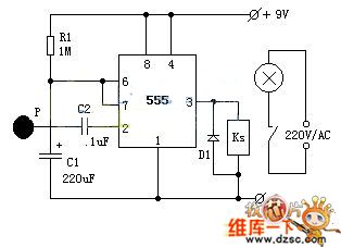
The integrated circuit IC1 is a piece of 555 timing circuit, connected to monostable circuit here. Usually as there's no induced voltage in the port of touching slab P, after the capacitance C1 passes 555 NO.7 pin to discharge, the outputof NO.3 pin is in low level, relay KS continue to release, the lamp won't be lighted.
While needing to turn on a lamp, to touch sheet metal P by hand, the human body's flooding wave signal voltage is applied into 555 triggering ports by C2, and makes 555 output change from low level to high level, the relay KS pulls in, the lamp will be turned on. At the same time, the interior of 555 NO. 7 pin stops working, the power supply then charges for C1 by R1, this is the periodic begin.When the voltage of C1 goes uo to 2/3 of power supply, 555 NO. 7 pin make C1 diacharge until NO. 3 pin is in low level again from high level, the relay releases, the lamp is turned off, this is the periodic over. (View)
View full Circuit Diagram | Comments | Reading(919)
Digital set type standard power supply circuit(CD4516, μA723C)diagram
Published:2011/3/22 21:55:00 Author:Rebekka | Keyword: Digital set type, standard power supply
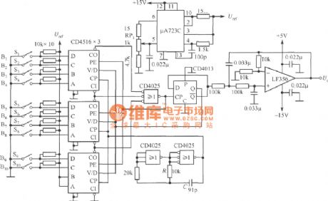
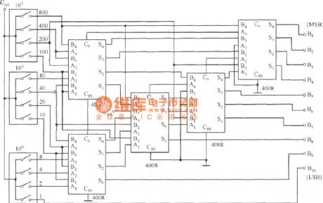
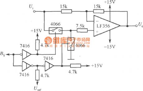
Digital set type standard power supply circuit diagram is shown as below. It is composed of digital set voltage switch(S1~S10), digital set type PWM circuit(CD4516, CD4025 and CD4013), smoothing PWM signal filter(LF356), clock generator(CD4025) and reference voltage source. Output voltage is set by Sl~S10, setting code is binary code. RPl is used for full-scale adjustment. Output voltage Uo will be adjusted to 10.23V when the digital input are all l. Filter gains 2 times(6dB), therefore, Uref is the half of 10.23V, voltage setting step is 10mV. To use the BCD-Binary number conversion circuit figure shown below when you use digital switch BCD code to set voltage. At this time, Uo is set to 3-digit display. The output voltage is 9.99V when the step voltage is 10mV.
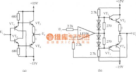
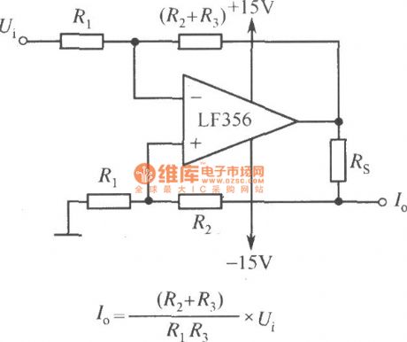
If you want to convert the polarity of output voltage, you can use the circuit diagram shown as below. The output Uo is positive voltage when Bs is 0; The output Uo is negative voltage when Bs is l. If you want to increase output power, you can use PA shown as the figure. But ±l5V power supply needs enough output power. If you want to change standard voltage into standard current source, you can add constant current circuit shown as the figure.
Output positive and negative voltage polarity converting circuit diagram:
PA circuit diagram:
Constant current circuit disgram:
(View)
View full Circuit Diagram | Comments | Reading(3250)
Light sensing circuit diagram
Published:2011/3/27 22:25:00 Author:Ecco | Keyword: Light sensing
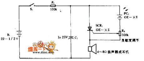
In the silicon-controlled trigger circuit, cadmium sulfide cell connects the relaxation oscillator before having a sensor to blink in darkroom. That make the speaker emit the warning sound of Ka, Li . The rate of the sound will increase with the quantity of light. When there is no blink, to modulate R2 until it's lower than the limiting value of sound. The circuitry is applied in fire warning system, and it uses the cadmium selenylation cell to replace PC1, as cadmium sulfide cell is more sensitive to infrared rays; when it's applied in temperature warning system, the optical spectrum expands to far infrared region, plumbum sulfide cell is applied in the circuitry as it is more sensitive to infrared rays.
(View)
View full Circuit Diagram | Comments | Reading(1903)
Step-down regulator circuit diagram composed of LM2579
Published:2011/3/28 4:34:00 Author:Nicole | Keyword: step-down regulator
View full Circuit Diagram | Comments | Reading(951)
Stepping motor and semi-conductor laser drive circuit diagram
Published:2011/3/28 4:24:00 Author:Nicole | Keyword: stepping motor drive, semi-conductor laser drive
View full Circuit Diagram | Comments | Reading(628)
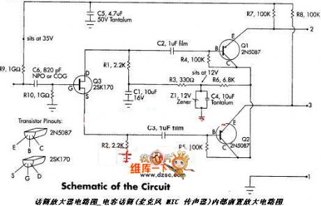
Microphone amplifier circuit diagram 1
Published:2011/3/25 1:48:00 Author:Ecco | Keyword: Microphone amplifier
Microphone amplifier circuit diagram 1 is as below:
(View)
View full Circuit Diagram | Comments | Reading(949)
7 ~ 30V adjustable output integrated voltage regulator circuit
Published:2011/3/24 23:07:00 Author:Joan | Keyword: 7 ~ 30V , adjustable output power supply , integrated voltage regulator
View full Circuit Diagram | Comments | Reading(720)
Microphone amplifier circuit diagram 2
Published:2011/3/25 1:49:00 Author:Ecco | Keyword: Microphone amplifier
View full Circuit Diagram | Comments | Reading(1104)
18V Monitoring circuit diagram
Published:2011/3/24 20:10:00 Author:Ecco | Keyword: Monitoring circuit
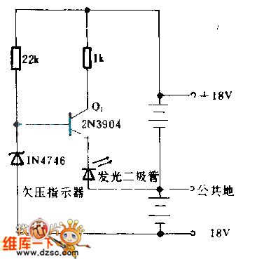
When ±18 V battery is discharged but cut to reserved low voltage, the Zener diode will be out of control, Q1's becoming is being positive-skew state, and the light-emitted diode needs to replace battery or refresh to them at this time. When the voltage of battery is normal, the Zener diode is placed in back bias state, the Q1 closes, and the light-emitted diode doesn't work and only consumes the current less than 1 mA. (View)
View full Circuit Diagram | Comments | Reading(873)
1/10/100 kb light receiving circuit diagram
Published:2011/3/28 21:24:00 Author:Ecco | Keyword: 1/10/100 kb light receiving
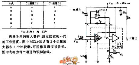
To choose different input components, the working velocity of receiving machine is different. The MC3405 in the figure including two operational amplifiers and two comparators, and it can be used as two channels receiver. The form in the figure is the pin connecting lines of each channel. (View)
View full Circuit Diagram | Comments | Reading(479)
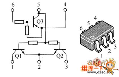
The inside circuit diagram of MMBT6427LT1 crystal triode
Published:2011/3/20 22:52:00 Author:Ecco | Keyword: MMBT6427LT1 crystal triode
The inside circuit diagram of MMBT6427LT1 crystal triode is as below:
(View)
View full Circuit Diagram | Comments | Reading(521)
The inside circuit diagram of crystal triode NUS2401SNT1
Published:2011/3/22 1:13:00 Author:Ecco | Keyword: crystal triode
The inside circuit diagram of crystal triode NUS2401SNT1 is as below:
(View)
View full Circuit Diagram | Comments | Reading(482)
The white LED drive circuit diagram with TL499A
Published:2011/3/24 21:59:00 Author:Ecco | Keyword: white LED drive
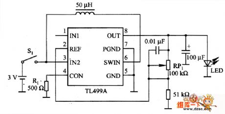
Here is the chart of the white LED drive circuit diagram with TL499A. The voltage of white LED drives is about 3.6V. If supplied common battery, it needs boosting circuitry composing of TL499A. TL499A is a type of adjustable output voltage integrated voltage regulation, and switching (voltage) regulator and linear regulator type can change automaticly when rising in switching (voltage) regulator type and descending in linear regulator type. The input voltage has a wide range of 1·1一10V(the switch works), the maximum is 35V(linear regulator works); the output voltage has a wide range of 2·9一30V, the maximum current is 100mA. In the chart, the working supplied by 2 sections of batteries in series connection, the crest value of switching current Ip of TL449A's pin 4 is about 200mA when R1 is -500 Ω. The resistance is low while the output current is high, Ip will increase simultaneously. RP1 is used as adjusting the output voltage. (View)
View full Circuit Diagram | Comments | Reading(2058)
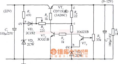
12V Collector output fixed power supply circuit diagram three
Published:2011/3/21 1:48:00 Author:Rebrecca | Keyword: Collector output, fixed power supply
View full Circuit Diagram | Comments | Reading(546)
15V、1A Collector output regulators power supply circuit diagram two
Published:2011/3/21 1:48:00 Author:Rebrecca | Keyword: Collector output, regulators power supply
15V、1A Collector output regulators power supply circuit diagram is shown as below.
(View)
View full Circuit Diagram | Comments | Reading(586)
1.45~15V Full sample fixed power supply circuit diagram
Published:2011/3/21 1:48:00 Author:Rebrecca | Keyword: Full sample , fixed power supply
View full Circuit Diagram | Comments | Reading(460)
The inside circuit diagram of PEMD10 crystal triode
Published:2011/3/20 22:52:00 Author:Ecco | Keyword: crystal triode
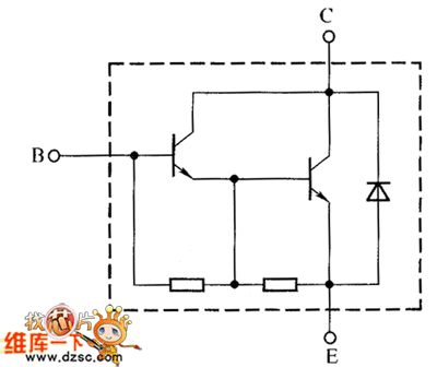
The inside circuit diagram of PEMD10 crystal triode is as below:
(View)
View full Circuit Diagram | Comments | Reading(495)
12V Collector output fixed power supply circuit diagram one
Published:2011/3/21 1:48:00 Author:Rebrecca | Keyword: Collector output , fixed power supply
View full Circuit Diagram | Comments | Reading(643)
Beelink tumbling-type massor circuit diagram
Published:2011/3/20 22:51:00 Author:Ecco | Keyword: tumbling-type massor
Beelink tumbling-type massor circuit diagram is as below:
(View)
View full Circuit Diagram | Comments | Reading(549)
| Pages:2210/2234 At 2022012202220322042205220622072208220922102211221222132214221522162217221822192220Under 20 |
Circuit Categories
power supply circuit
Amplifier Circuit
Basic Circuit
LED and Light Circuit
Sensor Circuit
Signal Processing
Electrical Equipment Circuit
Control Circuit
Remote Control Circuit
A/D-D/A Converter Circuit
Audio Circuit
Measuring and Test Circuit
Communication Circuit
Computer-Related Circuit
555 Circuit
Automotive Circuit
Repairing Circuit