
Circuit Diagram
Index 2214
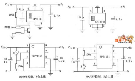
SPT1141/1151 Multifunction switch controller circuit diagram
Published:2011/3/22 1:00:00 Author:Nicole | Keyword: switch controller
View full Circuit Diagram | Comments | Reading(1053)
Ordinary transistor switching power supply circuit diagram
Published:2011/3/23 20:36:00 Author:Nicole | Keyword: transistor, switching power supply
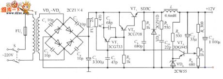
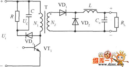
Transistor switching power is widely applied, as shown, this is a circuit diagram. In the figure, the transformer T, diodes VD1 ~ VD4 and capacitor C5 form the rectifier filter circuit; resistors R7, R8 and R9 in series sampling circuit; transistor VT4 as the error amplifier; transistor VT2, VT3 composite component switching regulator; VT1 is the pulse width adjustment tube; VT1, VT2, VT3 and the R3, C8 form the self-oscillation circuit; resistor R6 and Zener diode VD6 form reference; VD5 is the freewheeling diode; L is the energy storage inductor; VD5, L and C12 component output filter; R5 and C10 form a loop, it can make the freewheeling diode VD5 has good recovery characteristics.
(View)
View full Circuit Diagram | Comments | Reading(3063)
Regulator circuit diagram with input and output voltages only lV apart
Published:2011/3/28 2:36:00 Author:Nicole | Keyword: regulator
View full Circuit Diagram | Comments | Reading(595)
Single-ended flyback switching power supply circuit diagram of capacitance-type pressure clamp
Published:2011/3/22 21:48:00 Author:Nicole | Keyword: switching power supply
As shown, when the VT1 turns on, charging capacitor C02, C01 discharging, the primary winding N11 of the transformer Tl is applied to about l / 2 of the input voltage; when VTl stops, the voltage of N11 is polarity reversal, the emitter voltage Uce1 of VT1 reach the input voltage Ui, the diode VD4 turns on, Ucel is clamped; Similarly, VT2 turns on, C02 discharging, C01 charging, the primary winding N21 of T2 is applied to about 1 / 2 of the input voltage; VT2 stops, the voltage of N21 is polarity reversal, after VD3 turns on , Uce2 is also clamped to the input voltage Ui.
(View)
View full Circuit Diagram | Comments | Reading(759)
Single-ended forward converter circuit diagram with RC and diode clamp
Published:2011/3/24 3:09:00 Author:Nicole | Keyword: converter, RC, diode clamp
View full Circuit Diagram | Comments | Reading(931)
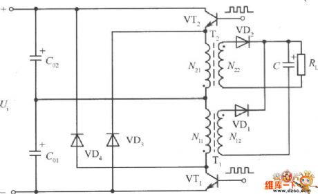
Double-ended converting circuit switching power supply circuit diagram
Published:2011/3/22 21:24:00 Author:Nicole | Keyword: switching power supply
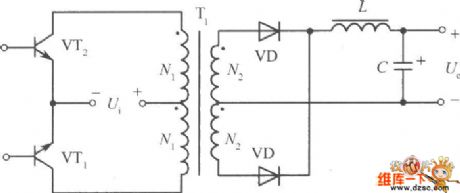
Push-pull converter is double-ended converter. The high-frequency transformer work both sides of the hysteresis loop, it is a simple design and reasonable line for a wide application. The typical circuit as shown. Switching transistor VTl, VT2 turned on and off by the base drive circuit alternating incentive, inputing DC voltage Ui converted into high frequency square wave AC voltage. VTl turns on, Ui through VT1 added to the primary winding Nl of the transformer T1. Due to the role of the transformer, the cut-off transistor VT2 will be imposed on 2 times input voltage, that is 2Ui. When the base incentive disappears, VTl, VT2 tubes are closed. The collector voltage is input voltage Ui. Next half cycle, VT2 turn on, VT1 stop, VTl 2 is imposed on 2 times input voltage, followed by another two cut-off, the next cycle to start again. The main disadvantage of push-pull circuit is the voltage of switching transistor should reach 2 times of the input power. The peak voltage, take the network voltage of 220 (1 ± 10%) V for example, the maximum steady cut-off voltage is 680V, coupled with the dynamic process of voltage spikes, switching transistors have to withstand more than 800V voltage.
(View)
View full Circuit Diagram | Comments | Reading(2114)
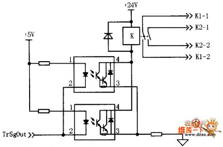
Dual optocoupler drive circuit diagram
Published:2011/3/28 2:23:00 Author:Nicole | Keyword: dual optocoupler drive
View full Circuit Diagram | Comments | Reading(743)
IC card interface and solenoid valve drive circuit diagram
Published:2011/3/28 2:14:00 Author:Nicole | Keyword: IC card interface, solenoid valve drive
View full Circuit Diagram | Comments | Reading(1223)
MOS switch tube drive circuit diagram
Published:2011/3/28 2:20:00 Author:Nicole | Keyword: switch tube drive
View full Circuit Diagram | Comments | Reading(644)
Cut-off reverse bias drive circuit diagram of unipolar pulse transformer
Published:2011/3/28 2:18:00 Author:Nicole | Keyword: reverse bias drive, unipolar pulse transformer
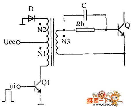
View full Circuit Diagram | Comments | Reading(1096)
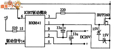
Power MOSFET drive circuit diagram
Published:2011/3/28 2:19:00 Author:Nicole | Keyword: Power MOSFET drive

View full Circuit Diagram | Comments | Reading(774)
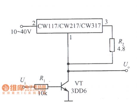
High-gain amplifier composed of CW117 circuit
Published:2011/3/28 2:23:00 Author:Joan | Keyword: High-gain amplifier
View full Circuit Diagram | Comments | Reading(550)
AC peak clipping composed of CW117 circuit
Published:2011/3/28 2:20:00 Author:Joan | Keyword: AC peak clipping
View full Circuit Diagram | Comments | Reading(577)
12V constant voltage charger composed of CW117 circuit
Published:2011/3/28 2:02:00 Author:Joan | Keyword: 12V , constant voltage charger
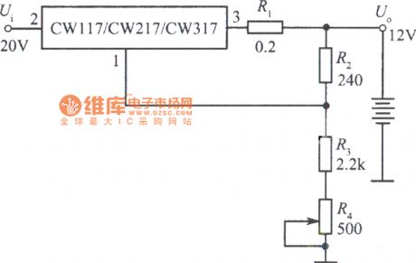
View full Circuit Diagram | Comments | Reading(554)
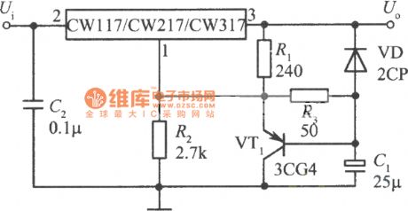
Slow start integrated voltage regulator circuit
Published:2011/3/28 2:00:00 Author:Joan | Keyword: Slow start , integrated voltage regulator
View full Circuit Diagram | Comments | Reading(957)
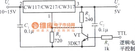
Logic control integrated voltage regulator circuit
Published:2011/3/28 1:59:00 Author:Joan | Keyword: Logic control , integrated voltage regulator
View full Circuit Diagram | Comments | Reading(545)
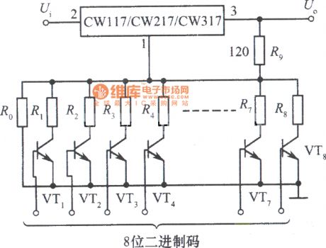
Digital control adjustable integrated voltage regulator circuit
Published:2011/3/28 1:58:00 Author:Joan | Keyword: Digital control , adjustable , integrated voltage regulator
View full Circuit Diagram | Comments | Reading(755)
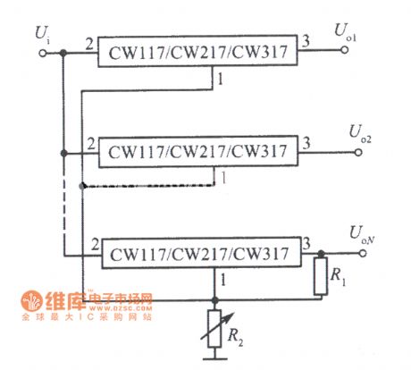
Multiple centralized control adjustable integrated voltage regulator circuit
Published:2011/3/28 1:49:00 Author:Joan | Keyword: Multiple , centralized control , adjustable , integrated voltage regulator
View full Circuit Diagram | Comments | Reading(605)
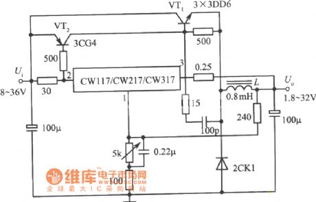
Switching integrated voltage regulator with 4A output current circuit
Published:2011/3/25 2:13:00 Author:Joan | Keyword: Switching integrated voltage regulator , 4A output current
View full Circuit Diagram | Comments | Reading(579)
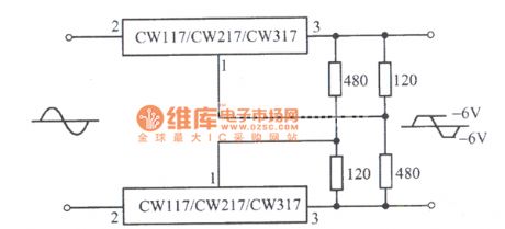
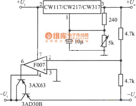
Positive and negative output voltage tracking integrated voltage regulator circuit 1
Published:2011/3/25 2:09:00 Author:Joan | Keyword: Positive and negative output voltage , tracking integrated voltage regulator
View full Circuit Diagram | Comments | Reading(707)
| Pages:2214/2234 At 2022012202220322042205220622072208220922102211221222132214221522162217221822192220Under 20 |
Circuit Categories
power supply circuit
Amplifier Circuit
Basic Circuit
LED and Light Circuit
Sensor Circuit
Signal Processing
Electrical Equipment Circuit
Control Circuit
Remote Control Circuit
A/D-D/A Converter Circuit
Audio Circuit
Measuring and Test Circuit
Communication Circuit
Computer-Related Circuit
555 Circuit
Automotive Circuit
Repairing Circuit