
Circuit Diagram
Index 36
Composed of integrated speed sensor KMI15/16 speed measuring circuit diagram
Published:2014/1/14 20:18:00 Author:lynne | Keyword: Composed of integrated speed sensor KMI15/16 speed measuring circuit diagram,
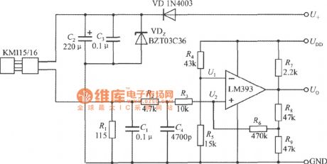
Composed of integrated speed sensor KMI15/16 speed measuring circuit diagram as shown:
(View)
View full Circuit Diagram | Comments | Reading(1274)
Reduce excitation voltage circuit (wideband strain signal conditioner 1B31) circuit diagram
Published:2014/1/14 20:09:00 Author:lynne | Keyword: Reduce excitation voltage circuit (wideband strain signal conditioner 1B31) circuit diagram,
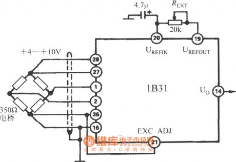
Reduce excitation voltage circuit (wideband strain signal conditioner1B31) circuit diagram shown in Fig.:
(View)
View full Circuit Diagram | Comments | Reading(895)
Noise Gate Noise Gate circuit diagram
Published:2014/1/14 18:31:00 Author: | Keyword: Noise Gate Noise Gate circuit diagram,
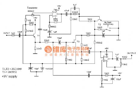
Noise Gate (door) Noise, the Noise of the door design to be in the absence of signal input, can remove Noise, and when a signal is input, covers signal to Noise.
As shown, whose Gate Noise Gate circuit diagram
(View)
View full Circuit Diagram | Comments | Reading(2913)
Equalizer circuit diagram
Published:2014/1/14 18:25:00 Author: | Keyword: Equalizer circuit diagram,
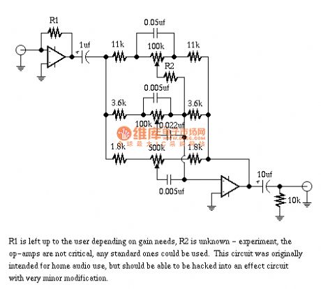
Equalizer circuit diagram as shown (View)
View full Circuit Diagram | Comments | Reading(1248)
Reverberation diagram
Published:2014/1/14 18:24:00 Author: | Keyword: Reverberation diagram,
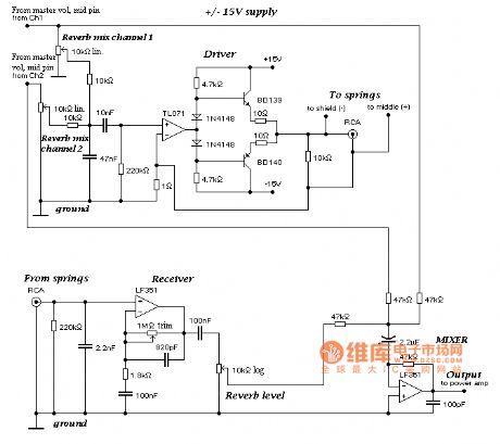
Reverberation diagram as shown (View)
View full Circuit Diagram | Comments | Reading(1054)
Article 20 the beam of light line display device driver circuit diagram
Published:2014/1/14 18:22:00 Author: | Keyword: Article 20 the beam of light line display device driver circuit diagram,
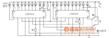
Article 20 the beam of light line display device driver circuit diagram
(View)
View full Circuit Diagram | Comments | Reading(983)
D2025 dual channel audio amplifier circuit diagram
Published:2014/1/14 18:21:00 Author: | Keyword: D2025 dual channel audio amplifier circuit diagram, D2025, DIP16
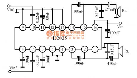
D2025 dual-channel audio power amplifier circuit D2025 stereo audio power amplifier integrated circuits for power amplifier using DIP16 package applicable to all types of portable tape recorders or portable stereo. Suitable for dual symmetrical or BTL wide-range supply voltage connections (3V ~ 12V) Maximum voltage gain 45dB (can be adjusted by an external resistor 3V low pressure under normal use.
As shown D2025 dual-channel audio amplifier circuit diagram
(View)
View full Circuit Diagram | Comments | Reading(5464)
D2003 power amplifier circuit diagram
Published:2014/1/13 22:17:00 Author: | Keyword: D2003 power amplifier circuit diagram,
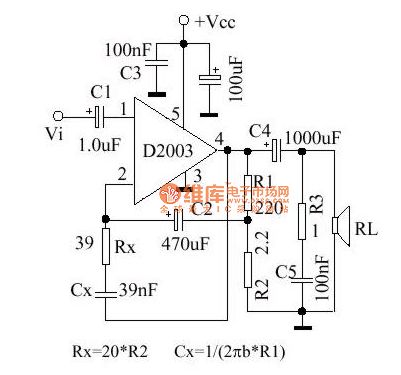
D2003 power amplifier circuit diagram as shown (View)
View full Circuit Diagram | Comments | Reading(1324)
Santana 2000GSi car central control door locks, rear window defroster circuit diagram
Published:2014/1/13 18:36:00 Author: | Keyword: Santana 2000GSi car central control door locks, rear window defroster circuit diagram,
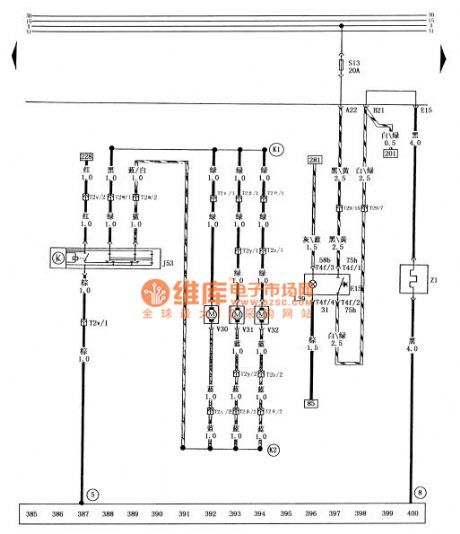
Tusangtana 2000GSi sedan centralized control door locks, rear window defroster circuit diagram
E15- rear window defroster switch J53- controlled lock controller L39- set rear window defroster switch lights rear window defroster S13- fuse (20A) T2v- left front door lock set additional control wiring harness and set central locking harness plug connector ( 2-pin in the front left door ) T2w- left front door lock set additional controls and centralized control door lock harness harness plug connector ( 2-pin in the front left door ) T2x- right front door lock set additional control wiring harness connection ( 2-pin , in the right front door ) and centralized control door lock harness plugs T2y- left rear door locks additional set of harness and left rear door attached harness plug connector ( 2-pin in the left rear door ) T2z- right rear door locks additional set Additional wiring harness and right rear door harness plug connector ( 2-pin , in the right rear door ) T2β- attach the harness and set the left rear door locks harness plug connector ( 2-pin , on the outside of the driver's seat under the carpet ) T2θ- attach the harness and set the right rear door lock harness plug connector ( 2-pin , in the passenger seat carpet outside ) T4f- dashboard switch harness with rear window defroster switch plug connector ( 4-pin on the rear window defroster switch ) T29- dashboard harness and instrument panel switch harness plug connector ( 29 -pin , at the bottom of the instrument cluster ) V30- set locks the front right , rear left set the motor V31- V32- controlled lock the right set of motor control motor Z1- lock rear window defroster ⑤ - ground ( on the right paw central star ground on the circuit board ) ⑧ - ground ( in the left rear combination lamps left the car body ) K1- cable ( in the central control door lock harness ) K2- cable ( the set Central locking wiring harness ) (View)
View full Circuit Diagram | Comments | Reading(1152)
Typical application circuit diagram TDA2616 audio power amplifier circuit
Published:2014/1/13 18:35:00 Author: | Keyword: Typical application circuit diagram TDA2616 audio power amplifier circuit, TDA2616
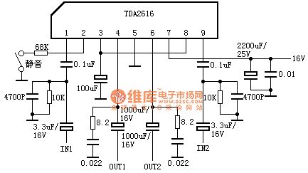
TDA2616 pin functions and reference voltage:
1 Foot: 10V - Signal Input 1
2 Feet: 5V - Squelch (low squelch)
3 Feet: 10V - 1/2 reference voltage
4 Feet: 10V - Signal output 1
5 feet: 0V - ground
6 Feet: 10V - Signal output 2
7 Feet: 20V - Power
8 feet: 10V - negative inputs
9 feet: 10V - Signal Input 2
Application Notes TDA2616 audio amplifier circuit shown in Figure typical
(View)
View full Circuit Diagram | Comments | Reading(11169)
Light type pulse tester circuit diagram
Published:2014/1/13 18:32:00 Author: | Keyword: Light type pulse tester circuit diagram

Light type pulse tester circuit diagram
(View)
View full Circuit Diagram | Comments | Reading(875)
NE5532 ore radio amplifier circuit diagram
Published:2014/1/13 18:30:00 Author: | Keyword: NE5532 ore radio amplifier circuit diagram, NE5532
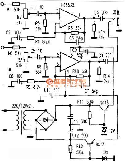
NE5532 ore radio amplifier circuit diagram as shown (View)
View full Circuit Diagram | Comments | Reading(2110)
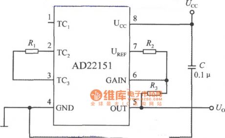
Single polarity mode of temperature compensation circuit diagram composed of linear output integrated magnetic field sensor AD22151
Published:2014/1/13 20:11:00 Author:lynne | Keyword: Single polarity mode of temperature compensation circuit diagram composed of linear output integrated magnetic field sensor AD22151,
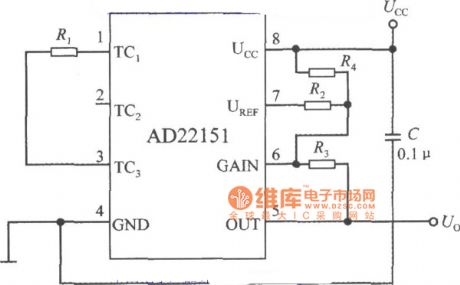
Single polarity mode of temperature compensation circuit diagram composed of linear output integrated magnetic field sensor AD22151 as shown:
(View)
View full Circuit Diagram | Comments | Reading(1043)
Bipolar mode of temperature compensation circuit diagram two composed of the integration of the linear output magnetic field sensor AD22151
Published:2014/1/13 20:14:00 Author:lynne | Keyword: Bipolar mode of temperature compensation circuit diagram two composed of the integration of the linear output magnetic field sensor AD22151,
Bipolar mode of temperature compensation circuit diagram two composed of the integration of the linear output magnetic field sensorAD22151 as shown in figure:
(View)
View full Circuit Diagram | Comments | Reading(1043)
Application circuit diagram of the biaxial magnetic field sensor with S/R and serial interface circuit
Published:2014/1/13 20:18:00 Author:lynne | Keyword: Application circuit diagram of the biaxial magnetic field sensor with S/R and serial interface circuit,
Application circuit diagram of the biaxial magnetic field sensor with S/R and serial interface circuitas shown:
(View)
View full Circuit Diagram | Comments | Reading(894)
Generate S / R (set / reset) pulse circuit (integrated magnetic sensor HMC1001/1002) circuit
Published:2014/1/13 20:20:00 Author:lynne | Keyword: Generate S / R (set / reset) pulse circuit (integrated magnetic sensor HMC1001/1002) circuit,
Generate S / R (set / reset) pulse circuit (integrated magnetic sensor HMC1001/1002) circuit shown in Figure:
(View)
View full Circuit Diagram | Comments | Reading(1033)
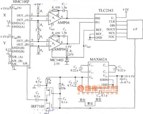
Dual-axis magnetic field sensor application circuit with S / R circuit and serial interface (integrated magnetic sensor HMC1002) circuit diagram
Published:2014/1/13 20:21:00 Author:lynne | Keyword: Dual-axis magnetic field sensor application circuit with S / R circuit and serial interface (integrated magnetic sensor HMC1002) circuit diagram,
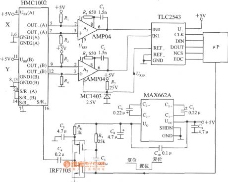
Dual-axis magnetic field sensor application circuit with S / R circuit and serial interface (integrated magnetic sensor HMC1002) circuit diagram shown in Fig.:
(View)
View full Circuit Diagram | Comments | Reading(2349)
Human body reaction velocity tester circuit diagram
Published:2014/1/13 0:59:00 Author: | Keyword: Human body reaction velocity tester circuit diagram,
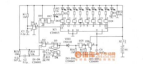
Human body reaction velocity tester circuit diagram
The human body reaction speed tester circuit as shown. Nand gate D25, D26 multivibrator, the output clock pulse cycle of about 50 ms. IC1 composed of eight moves to the right register, boot of D1 delay circuit output signal as a serial input data. Just when switched on, because of the D1 output is 1 , under the effect of clock pulse, the IC1 8-bit register unit quickly for all 1 ; After 3 ~ 4 s s, D1 output into a 0 , the test lamp VD1 bright, at the same time, the IC1 8-bit register units will be under the effect of clock pulse from left to right in turn into a 0 , until they are testing people press the stop button S1, D3, D4 RS flip-flop consisting of 0 , make the D25, D26 stop, keep IC1, the result through the drive circuit D13 ~ D16, D21 ~ D24 drive led display. D2 role is to make the stop button S1 only after the test signal VD1 light works, press ahead is invalid. (View)
View full Circuit Diagram | Comments | Reading(1316)
Typical application circuit diagram TDA2009 audio power amplifier circuit
Published:2014/1/13 0:55:00 Author: | Keyword: Typical application circuit diagram TDA2009 audio power amplifier circuit, TDA2009
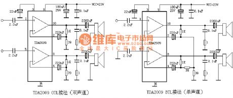
TDA2009
1-Foot: 1.2V-- Left channel input
2-Feet: 0.8V-- Left channel feedback
3 Feet: 12V - Squelch
4-Feet: 0.8V-- right channel feedback
5 Feet: 1.2V-- right channel input
6 Feet: 0V - ground
7 Feet: 0V - empty
8 feet: 12.4V-- right channel output
9 feet: 24V - Power
10 feet: 12.4V-- Left channel output
Application Notes TDA2009 audio amplifier circuit shown in Figure typical
(View)
View full Circuit Diagram | Comments | Reading(1969)
Typical application circuit diagram TDA1521 audio power amplifier circuit
Published:2014/1/13 0:38:00 Author: | Keyword: Typical application circuit diagram TDA1521 audio power amplifier circuit, TDA1521
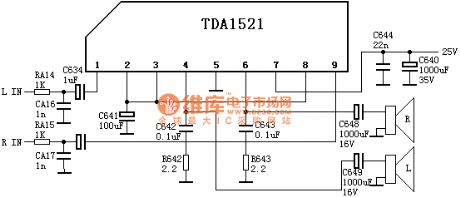
The circuit is taken from Changhong C2191, dual-channel access method for the OTL.
TDA1521 pin functions and reference voltage:
1 foot: 11V - Reverse Input 1 (L-channel signal input)
2 feet: 11V - Forward Input 13 feet: 11V - Reference 1 (when OCL connection to 0V, when OTL connection to 1/2Vcc)
4 feet: 11V - Output 1 (L-channel signal output)
5 feet: 0V - Negative power input (OTL connection when ground)
6 Foot: 11V - Output 2 (R channel signal output)
7 Foot: 22V - Positive power supply input
8 feet: 11V - positive input 2
9 feet: 11V - Reverse Input 2 (R-channel signal input)
Application Notes TDA1521 audio amplifier circuit shown in Figure typical
(View)
View full Circuit Diagram | Comments | Reading(3847)
| Pages:36/2234 At 202122232425262728293031323334353637383940Under 20 |
Circuit Categories
power supply circuit
Amplifier Circuit
Basic Circuit
LED and Light Circuit
Sensor Circuit
Signal Processing
Electrical Equipment Circuit
Control Circuit
Remote Control Circuit
A/D-D/A Converter Circuit
Audio Circuit
Measuring and Test Circuit
Communication Circuit
Computer-Related Circuit
555 Circuit
Automotive Circuit
Repairing Circuit