
Circuit Diagram
Index 22
ICETEK C6711 -- A schematic diagram 4
Published:2014/2/24 21:40:00 Author: | Keyword: ICETEK C6711 -- A schematic diagram 4,
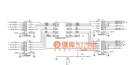
As shown in figure ICETEK C6711 -- A principle diagram 4 (View)
View full Circuit Diagram | Comments | Reading(751)
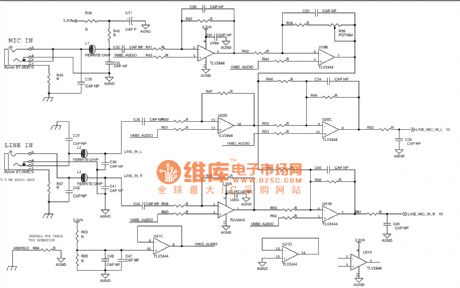
DZW75-48/50 (ii) 50 are filled, floating conversion circuit diagram
Published:2014/2/24 21:24:00 Author: | Keyword: DZW75-48/50 (ii) 50 are filled, floating conversion circuit diagram,
View full Circuit Diagram | Comments | Reading(744)
ICETEK C6711 -- A schematic 05
Published:2014/2/24 21:17:00 Author: | Keyword: ICETEK C6711 -- A schematic 05,

As shown ICETEK C6711 -- A schematic 05 (View)
View full Circuit Diagram | Comments | Reading(816)
Damp, cool alarm circuit
Published:2014/2/24 20:23:00 Author:lynne | Keyword: Damp, cool alarm circuit,
Damp, cool alarm circuit shown in Figure:
(View)
View full Circuit Diagram | Comments | Reading(989)
Dongfeng Peugeot Citroen Picasso heating ventilation circuit
Published:2014/2/24 20:23:00 Author:lynne | Keyword: Dongfeng Peugeot Citroen Picasso heating ventilation circuit,
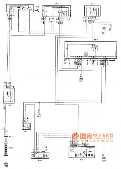
Dongfeng Peugeot Citroen Picasso heating ventilation circuit shown in Figure:
(View)
View full Circuit Diagram | Comments | Reading(1116)
Dongfeng Peugeot Citroen Picasso 2.0L Front and rear fog lamps circuit
Published:2014/2/24 20:20:00 Author:lynne | Keyword: Dongfeng Peugeot Citroen Picasso 2.0L Front and rear fog lamps circuit,
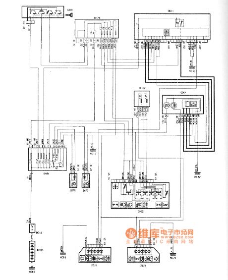
Dongfeng Peugeot Citroen Picasso 2.0L Front and rear fog lamps circuit shown in Figure:
(View)
View full Circuit Diagram | Comments | Reading(3169)
1.2 V voltage could be turned into 9 V converter circuit diagram
Published:2014/2/24 20:16:00 Author:lynne | Keyword: 1.2 V voltage could be turned into 9 V converter circuit diagram,
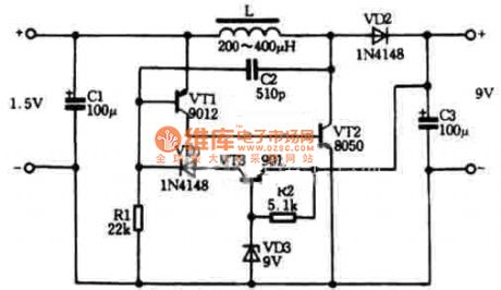
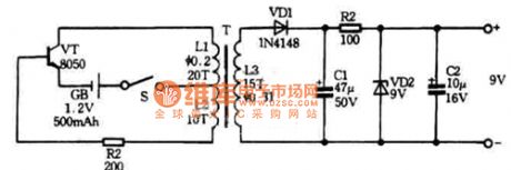
Figure 1 is a DC voltage boost circuit. The circuit can be a boost to 1.5V battery 9V, 9V laminated battery to replace. Circuit load input current is less than 1.2mA, the conversion efficiency up to 60%. The circuit consists of an oscillation circuit and voltage regulator circuit, which VT1, VT2, C2 composition oscillator, color code inductance L is the inductor, VD2 rectifier diode, C3 is the output filter capacitor, VT3, VD1, VD3 and R2 is stable the output voltage of the voltage regulator circuit. The output voltage is approximately equal to the value of VD3 of regulator. DC boost regulator circuit diagram shown in Figure 1
Figure 2 is a use of 1.2V, 500mAh nickel-cadmium batteries do power inverter circuit, the output voltage of 9V, digital multimeter available for use. Power inverter circuit shown in Figure 2
(View)
View full Circuit Diagram | Comments | Reading(4873)
Single-chip infrared sensor controller ZH9576 and application circuit diagram
Published:2014/2/24 20:13:00 Author:lynne | Keyword: Single-chip infrared sensor controller ZH9576 and application circuit diagram,
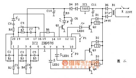
Single-chip infrared sensor controller ZH9576 and application circuit diagram as shown:
(View)
View full Circuit Diagram | Comments | Reading(940)
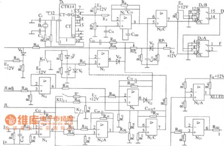
DZW75-48/50 (50 ii) voltage and current limit, flow diagram
Published:2014/2/23 21:27:00 Author: | Keyword: DZW75-48/50 (50 ii) voltage and current limit, flow diagram,
View full Circuit Diagram | Comments | Reading(857)
ICETEK C6711 -- A principle diagram of 06
Published:2014/2/23 21:25:00 Author: | Keyword: ICETEK C6711 -- A principle diagram of 06,
As shown in figure ICETEK C6711 -- A principle diagram of 06 (View)
View full Circuit Diagram | Comments | Reading(771)
Blown fuse flash circuit diagram
Published:2014/2/23 21:24:00 Author: | Keyword: Blown fuse flash circuit diagram,
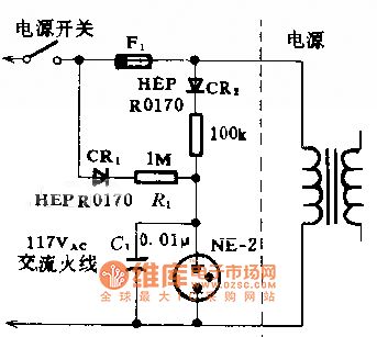
Blown fuse flash circuit diagram
(View)
View full Circuit Diagram | Comments | Reading(881)
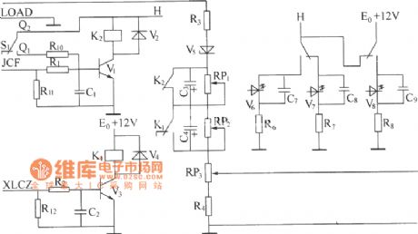
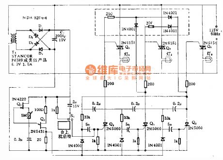
DZW75-48/50 (ii) 50 high-frequency rectifier filter circuit diagram
Published:2014/2/23 21:18:00 Author: | Keyword: DZW75-48/50 (ii) 50 high-frequency rectifier filter circuit diagram,
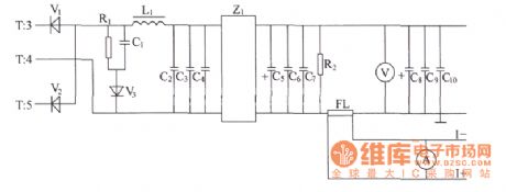
High-frequency transformer T secondary induction of positive and negative pulse of alternating voltage, after composed of high-power high-frequency switching diode V1 and V2 full-wave rectifier rectifier, repass L1 inductor and capacitor C2, C3 and C4 L filter and Z1 power filter consisting of smoothing filtering, such as on the output side for high frequency noise in accordance with the requirements of the indicators of 48 v dc voltage output. Pulse width directly decided to the discretion of the output voltage. Pulse width is wide, the output voltage is high, narrow pulse width, low output voltage. On the output side and a voltmeter, to display the output dc voltage measurement. R2 for discharge resistance, FL for shunt, a current meter jumper on both ends of FL to measure shows that the output of the rectifier current value, voltage value at the ends of the FL also as output current sampling signal to the voltage and current limit, flow circuit. R1, C1 and V3 RCD absorbing circuit to absorb the secondary voltage overshoot. (View)
View full Circuit Diagram | Comments | Reading(864)
The trigger drive SCR flash circuit diagram
Published:2014/2/23 21:13:00 Author: | Keyword: The trigger drive SCR flash circuit diagram,
The trigger drive SCR flash circuit diagram
(View)
View full Circuit Diagram | Comments | Reading(1208)
ICETEK 07 - C6711 - A schematic diagram
Published:2014/2/23 21:12:00 Author: | Keyword: ICETEK 07 - C6711 - A schematic diagram,
As shown in figure ICETEK 07 - C6711 - A schematic diagram (View)
View full Circuit Diagram | Comments | Reading(759)
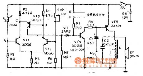
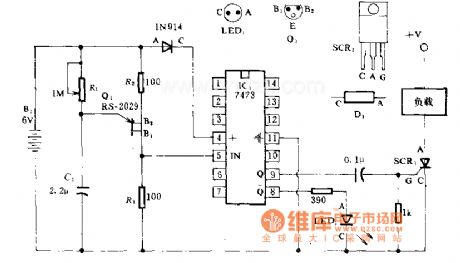
1.5 v led flash circuit diagram
Published:2014/2/23 21:10:00 Author: | Keyword: 1.5 v led flash circuit diagram,
1.5 v led flash circuit diagram
(View)
View full Circuit Diagram | Comments | Reading(1107)
Order book flash communication circuit diagram
Published:2014/2/23 21:08:00 Author: | Keyword: Order book flash communication circuit diagram,
Order book flash communication circuit diagram
(View)
View full Circuit Diagram | Comments | Reading(926)
DZW75-48/50 (ii) 50 drive circuit diagram
Published:2014/2/23 21:04:00 Author: | Keyword: DZW75-48/50 (ii) 50 drive circuit diagram,
View full Circuit Diagram | Comments | Reading(831)
ICETEK C6711 -- A principle chart 08
Published:2014/2/23 21:01:00 Author: | Keyword: ICETEK C6711 -- A principle chart 08,
As shown in figure ICETEK C6711 -- A principle chart 08 (View)
View full Circuit Diagram | Comments | Reading(858)
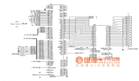
DZW75-48/50 (ii) 50 input circuit diagram
Published:2014/2/23 20:51:00 Author: | Keyword: DZW75-48/50 (ii) 50 input circuit diagram,
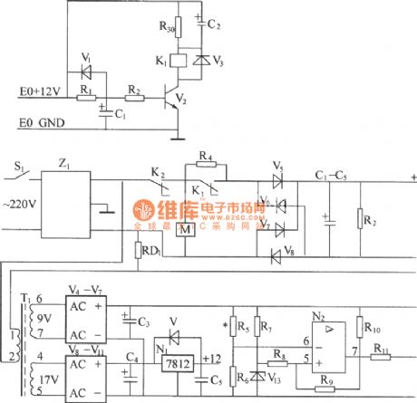
(1) 220 v AC voltage (50 hz) after Z1 line filter filter to AC overvoltage, undervoltage protection relay K2 contact, K2 contacts shall be closed up in normal working conditions, the AC voltage from 220 v AC current limiting resistor R4 R4 (after startup delay a period of time by K1 contact nipple), sent to the bridge rectifier rectifier power frequency, after smoothing filter and capacitor group about the output voltage of the DC 300 v, AC/DC power frequency conversion. R2 for discharge resistor. (2) the Z1 line filter is used to suppress and absorption power grid may have strong pulse interference with rectifier, improve the reliability of the rectifier. Line filter is good at the same time the common mode and differential mode of insertion loss, can effectively suppress the high frequency switch converter produced by reverse output of high frequency interference signals, the rectifier and isolation of power network, avoid mutual interference. (3) ac overvoltage, undervoltage protection circuit, ac 220 v voltage of line filter filter to the step-down transformer. (4) ac current limit delay circuit, ac voltage within the normal working range can be connected to the machine, ac power after the access time in auxiliary power supply, and after the construction of the auxiliary power supply by time delay, to make communication sub resistor, this paragraph of time is called ac current limit delay, it is being done by the alternating current limit delay circuit. (View)
View full Circuit Diagram | Comments | Reading(851)
ICETEK C6711 -- A schematic 09
Published:2014/2/23 20:45:00 Author: | Keyword: ICETEK C6711 -- A schematic 09,
As shown in figure ICETEK C6711 -- A schematic 09 (View)
View full Circuit Diagram | Comments | Reading(812)
| Pages:22/2234 At 202122232425262728293031323334353637383940Under 20 |
Circuit Categories
power supply circuit
Amplifier Circuit
Basic Circuit
LED and Light Circuit
Sensor Circuit
Signal Processing
Electrical Equipment Circuit
Control Circuit
Remote Control Circuit
A/D-D/A Converter Circuit
Audio Circuit
Measuring and Test Circuit
Communication Circuit
Computer-Related Circuit
555 Circuit
Automotive Circuit
Repairing Circuit