
Circuit Diagram
Index 37
Typical application circuit diagram TA8211AH audio power amplifier circuit
Published:2014/1/13 0:30:00 Author: | Keyword: Typical application circuit diagram TA8211AH audio power amplifier circuit, TA8211AH
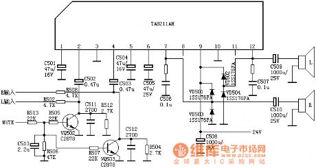
The circuit is taken from Changhong C2588-shaped TV
Pin 1: 2.1V-- Left channel negative feedback external capacitor
Pin 2: 2.2V-- left channel signal input
Pin 3: 0V - ground
Pin 4: 2.2V-- right channel signal input
Pin 5: 2.1V-- Right channel negative feedback external capacitor
Pin 6: 8.2V-- Power Filter
Pin 7: 12V - right channel signal output
Pin 8: 2.2V-- empty
Pin 9: 24V - Power
Pin 10: 2.2V-- empty
Pin 11: 12V - left channel signal output
Diagram TA8211AH typical audio amplifier circuit shown in Figure
(View)
View full Circuit Diagram | Comments | Reading(4693)
Typical application circuit diagram LA4287 audio power amplifier circuit
Published:2014/1/13 0:31:00 Author: | Keyword: Typical application circuit diagram LA4287 audio power amplifier circuit, LA4287
TV audio signal from ( 1 ) pin input N601 's , AV audio signal from ( 3 ) feet of the input N601 , CPU (40) pin output TV / AV switching signal via the base of R601 to V601 , V601 inverted by the after controlling N601 's ( 4 ) feet , after an internal selection ( 9 ) pin outputs an audio signal from the N601 , pushing the horn sound.
V641, V642 audio squelch circuit consisting shutdown : normal boot , 12V voltage is applied through R641 base V641 , V641 has been added to the emitter VD642 , VD642 because of the presence of so than the base -emitter voltage V641 high voltage 0.7V, V641 deadline , V642 also cut , this circuit has no effect on the volume control , then, the C641 is near the 12V charging voltage . After the shutdown , 12V voltage disappears , since the case is filled with the C641 12V voltage , so the base voltage V641 is lower than the emitter voltage , V641 conduction , V642 is also on, the volume control voltage is shorted to ground , to achieve a static off noise .LA4287 pin functions and reference voltage:
Pin 1 : 6.3V-- Signal Input 1
Pin 2 : 0V - ground
Pin3 6.3V-- Signal Input 2
Pin 4: 2.1V-- signal switch
Pin 5: 0.67V-- Volume control voltage input
Pin 6: 9.8V-- Filter
Pin 7: 9.8V-- Feedback
Pin 8: 0V - ground
Pin 9: 9.9V-- Output
Pin 10: 21V - Power
Diagram LA4287 typical audio amplifier circuit shown in Figure
(View)
View full Circuit Diagram | Comments | Reading(1688)
Isolated programmable voltage / current sensor 1B22 application in the pressure measurement system circuit diagram
Published:2014/1/12 21:45:00 Author:lynne | Keyword: Isolated programmable voltage / current sensor 1B22 application in the pressure measurement system circuit diagram,
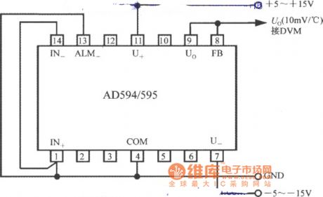
Isolated programmable voltage / current sensor 1B22 application in the pressure measurement system circuit diagram as shownin Figure:
(View)
View full Circuit Diagram | Comments | Reading(917)
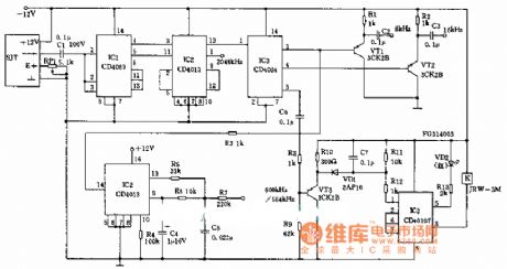
The second of the blind Pathfinders (μA741, LM567, KD153) circuit diagram
Published:2014/1/12 21:41:00 Author:lynne | Keyword: The second of the blind Pathfinders (μA741, LM567, KD153) circuit diagram,
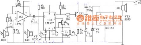
The secondof the blind Pathfinders (μA741, LM567, KD153)circuit diagramas shown:
(View)
View full Circuit Diagram | Comments | Reading(1348)
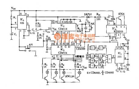
The first of the Blind Pathfinders (LM567, KD56022) circuit
Published:2014/1/12 21:40:00 Author:lynne | Keyword: The first of the Blind Pathfinders (LM567, KD56022) circuit,
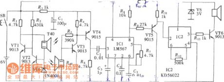
One of the Blind Pathfinders(LM567, KD56022) circuit shown in Figure:
(View)
View full Circuit Diagram | Comments | Reading(1320)
Train lights automatically switch circuit
Published:2014/1/12 21:37:00 Author:lynne | Keyword: Train lights automatically switch circuit,
Train lights automatically switch circuit shown in Figure:
(View)
View full Circuit Diagram | Comments | Reading(977)
SH type hole connected and the MOS circuit output interface circuit diagram
Published:2014/1/12 21:35:00 Author:lynne | Keyword: SH type hole connected and the MOS circuit output interface circuit diagram,
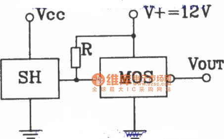
SH type hole connectedand the MOS circuit output interface circuit diagram as shown:
(View)
View full Circuit Diagram | Comments | Reading(802)
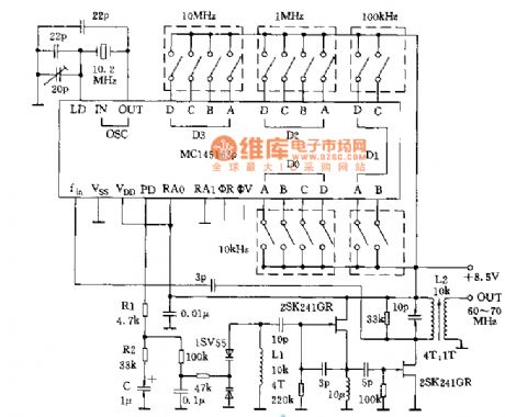
The frequency synthesizer circuit
Published:2014/1/9 20:37:00 Author:lynne | Keyword: The frequency synthesizer circuit,
The frequency synthesizer circuit shown in Figure:
(View)
View full Circuit Diagram | Comments | Reading(1580)
PLL frequency synthesizer schematic circuit
Published:2014/1/9 20:23:00 Author:lynne | Keyword: PLL frequency synthesizer schematic circuit,
PLL frequency synthesizer schematic circuit shown in Figure:
(View)
View full Circuit Diagram | Comments | Reading(2547)
Palio front and rear fog lamps circuit
Published:2014/1/9 20:20:00 Author:lynne | Keyword: Palio front and rear fog lamps circuit,
Palio frontand rear fog lamps circuit shown in Figure:
(View)
View full Circuit Diagram | Comments | Reading(855)
Palio turn lights and emergency lights circuit
Published:2014/1/9 20:18:00 Author:lynne | Keyword: Palio turn lights and emergency lights circuit,
Palio turn lights and emergency lights circuit shown in Figure:
(View)
View full Circuit Diagram | Comments | Reading(801)
Palio passenger compartment lamp circuit
Published:2014/1/9 20:16:00 Author:lynne | Keyword: Palio passenger compartment lamp circuit,
Palio passenger compartment lamp circuit shown in Figure:
(View)
View full Circuit Diagram | Comments | Reading(851)
Typical application circuit diagram AN5265 audio power amplifier circuit
Published:2014/1/9 20:01:00 Author: | Keyword: Typical application circuit diagram AN5265 audio power amplifier circuit, AN5265
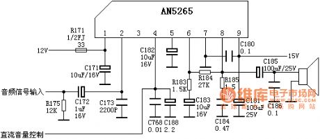
AN5265 pin functions and reference voltage:
Pin 1: 12V - Front-level power
Pin 2: 5V - audio signal input
Pin 3: 0V - Mute control terminal (high Mute)
Pin 4: 0.1V-- Volume control voltage input terminal
Pin 5: 7V - Filtering end
Pin 6: 7.4V-- Negative feedback input
Pin 7: 0V - ground
Pin 8: 7.5V-- the output of the power amplifier
Pin 9: 15V - power amplifier stage
Application Notes AN5265 typical audio amplifier circuit shown in Fig.
(View)
View full Circuit Diagram | Comments | Reading(4424)
Typical application circuit diagram LA4225A audio power amplifier circuit
Published:2014/1/9 19:58:00 Author: | Keyword: Typical application circuit diagram LA4225A audio power amplifier circuit, LA4225A
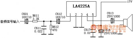
Diagram LA4225A typical audio amplifier circuit shown in Figure (View)
View full Circuit Diagram | Comments | Reading(1885)
Dual channel long-term transmission circuit diagram
Published:2014/1/9 19:54:00 Author: | Keyword: Dual channel long-term transmission circuit diagram,
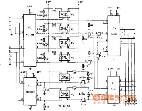
The main features of the long-term transmitter is input and output circuit adopts photoelectric isolation technology, computer and communication lines, communication lines between the terminal equipment and realized the complete electrical isolation. Can prevent the accident on line voltage, electromagnetic induction and jamming signal into the computer and terminal equipment, improve the common on sex and the stability of the computer.
This long-term transmitter circuit can work in the second half duplex or four-wire full-duplex two works. The transfer rate of 0-9, 600 - bit/s, using twisted-pair telephone transmission distance up to 10 km, at close range of computer communication, it can replace the modem.
Shown in the figure for the second line half duplex mode. At this point the first (4) (request) RS - 232 control channel to send and receive state. If it is the logic 1 is the channels for the state, or for the closed state.
If you want to work in four lines full duplex mode, as long as in the figure. A, b, c, d four thread off, and in CZ1 (1), (2), (3), (4) respectively after 1 300 Ω terminating resistance can, at this time without the RS - 232 in the first 4 request control signals. (View)
View full Circuit Diagram | Comments | Reading(905)
Photoelectric isolation type quick switch circuit diagram
Published:2014/1/9 19:46:00 Author: | Keyword: Photoelectric isolation type quick switch circuit diagram,
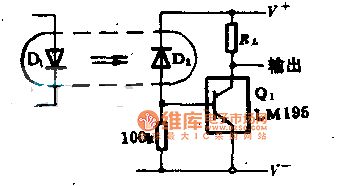
This circuit can use almost any standard of optoelectronic isolator. As long as the photoelectric diode D; Pick up to less than 20 mu A in the current, can make LM195 power transistor conduction, D2 of the cathode is power directly, and not be collector of Q1, to eliminate the influence of base - the collector capacitance. In 40 v, 1 A load case, the switch speed increased to 500 ns.
(View)
View full Circuit Diagram | Comments | Reading(723)
A 24 million - bit data circuit diagram
Published:2014/1/9 19:44:00 Author: | Keyword: A 24 million - bit data circuit diagram,
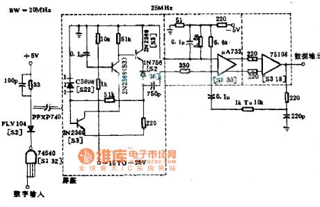
By improving the performance of the receiver, the digital output from the electric typewriter is a message on the far side of feed to the microprocessor, can achieve high data rate for square wave pulse. Pre set designed for use in a limited frequency range to compensate the noise, until about 20 MHZ, has uniform letter/noise ratio. In the demonstration device, the image method in visible light leds and photoelectric detector, at 19.2 cm (40 feet) long cable meet the requirements on its performance.
(View)
View full Circuit Diagram | Comments | Reading(832)
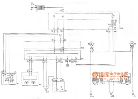
Palio headlamp beam adjustment device circuit
Published:2014/1/8 20:39:00 Author:lynne | Keyword: Palio headlamp beam adjustment device circuit,
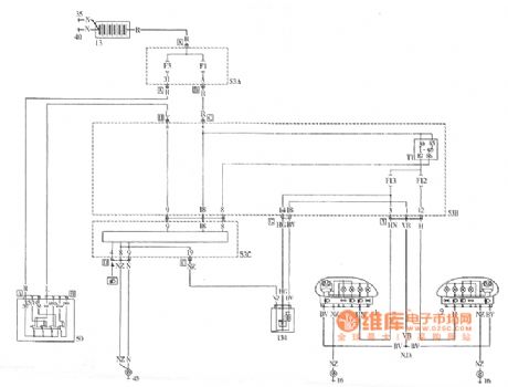
Palio headlamp beam adjustment device circuit shown in Figure:
(View)
View full Circuit Diagram | Comments | Reading(866)
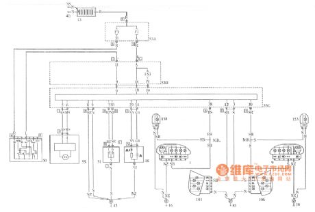
Palio windshield the after skylight windscreen wiper jetter- the after wind window heating
Published:2014/1/8 20:32:00 Author:lynne | Keyword: Palio windshield the after skylight windscreen wiper jetter- the after wind window heating,
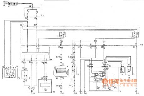
Palio windshield the afterskylightwindscreen wiper jetter- the after wind windowheating circuit diagram as shown:
(View)
View full Circuit Diagram | Comments | Reading(806)
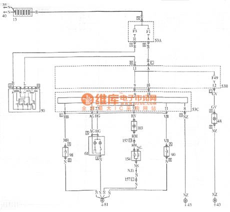
Palio cassette player system circuit diagram
Published:2014/1/8 20:25:00 Author:lynne | Keyword: Palio cassette player system circuit diagram,
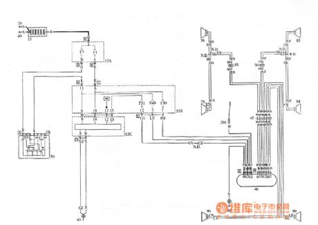
Palio cassette player system circuit diagram as shown:
(View)
View full Circuit Diagram | Comments | Reading(960)
| Pages:37/2234 At 202122232425262728293031323334353637383940Under 20 |
Circuit Categories
power supply circuit
Amplifier Circuit
Basic Circuit
LED and Light Circuit
Sensor Circuit
Signal Processing
Electrical Equipment Circuit
Control Circuit
Remote Control Circuit
A/D-D/A Converter Circuit
Audio Circuit
Measuring and Test Circuit
Communication Circuit
Computer-Related Circuit
555 Circuit
Automotive Circuit
Repairing Circuit