
power supply circuit
Index 16
Sound Effects Generator 3
Published:2013/7/30 20:40:00 Author:muriel | Keyword: Sound Effects Generator 3
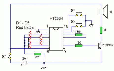
Notes:All sound effects are generated internally by the HT2884 IC. Power is a 3 Volt battery, but the IC will work with any voltage between 2.5 and 5 Volts. Switch S1 is the on / off switch. The output at pin 10 is amplified and drives a small 8 ohm loudspeaker. Pressing S3 once will generate all the sounds, one after another. S2 can be used to produce a single sound effect, next depression gives the next sound effect. There are 2 lazer guns, 1 dual tone horn sound, 2 bomb sounds, 2 machine gun sounds and a rifle shot sound. Standby current is about 1 uA at 3 Volt, so battery life is very economical. The IC may be obtained from Maplin Electronics order code AZ52G. (View)
View full Circuit Diagram | Comments | Reading(1003)
Sound Effects Generators
Published:2013/7/30 20:35:00 Author:muriel | Keyword: Sound Effects Generators
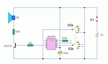
Notes:Nothing too complicated here. The IC produces all the sound effects, the output at Pin 3 being amplified by the transistor. A 64 ohm loudspeaker can be substituted in place of the 56 ohm resistor and 8 ohm loudspeaker. The 2 pole 4 way switch controls the sound effects. Position 1 (as drawn) being a Police siren, position 2 is a fire engine sound, 3 is an ambulance and position 4 is a machine gun effect. The IC is manufactured by UMC and was available from Maplin electronics code UJ45Y. At the time of writing this has now been discontinued, but they have have limited stocks available. (View)
View full Circuit Diagram | Comments | Reading(994)
Adjustable High/Low Frequency Sine wave generator
Published:2013/7/30 20:29:00 Author:muriel | Keyword: Adjustable , High/Low Frequency , Sine wave, generator
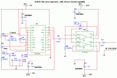
This circuit uses the versatile MAX038 function generator. Although in this circuit some of the advanced characteristics of this IC are disabled, you can generate Sine, Triangle, Square waves (adjusting A0 and A1 pins see datasheet on www.maxim-ic.com if you want other waves, use a switch).The signal is amplified through a TCA0372 (from ONSEMI) Power opamp with current capability up to 1A and bandwitch up to 1 MHz.I selected this particular frequency (122 Khz) because i needed a cheapo ESR-o-meter for my electrolytic capacitors to monitor their health as they have to discharge tens of amperes in less than 2 ms. At 122 KHz capacitive reactance is very low, and inductive reactance isn't so high, so forcing a current (es 200mA, using a precision resistor) through a capacitor and reading AC voltage drop accross it gives me an estimation of ESR (Vdrop/current). Of course inductive and capacitive reactance are still present, but negligible.Let's back to the circuit.
Operation:The 122 khz 2V p-p sine wave is generated by the MAX038 IC, its frequency can be calculated by the formula Freq (MHz) = Iin(uA) / C6 (pf) . Iin = 2,5V / R1 (25Kohm default). So the freq is 0,122 MHz . The resistor is for small adjustments, don't go under 10000 Kohm or above 40000 Kohm because the accuracy will drop. If you want multifrequency just use the multiposition switch with 820 pF, 8,2 nF , 82nF , 820 nf for 122Khz range 12,2Khz range 1220 Hz and 122 Hz. Fine tuning can be done adjusting R2 , the frequency can vary from 1,7x (Vfadj = -2,4) to 0,3x (Vfadj = 2,4) of the main frequency (when fadj is at 0V).The sine wave output is feed into a TCA0372 1/2 opamp to achieve a gain from 1 to 5 (2V p-p, 10 V p-p), adjust the potenziometer and into a TCA0372 2/2 opamp buffer stage also present on the same IC.
Important:Adjusting the frequency needs a frequency counter, so this circuit should be used on conjunction with a freq couter. The max current is 1A, but i would suggesto to not go above 0,5A to remain accurate. Needs a computer power supply with 12V,5V,-5V,-12V,GND to be operated, if you don't have one just use a multivoltage mains transformer (15 watt is enough) diode bridges (low current 1-2 Amps), smoothing capacitors 10000uF 16V, and voltage regulators such as LM7905 and LM7912. (View)
View full Circuit Diagram | Comments | Reading(1644)
Function Generators
Published:2013/7/30 20:29:00 Author:muriel | Keyword: Function Generators
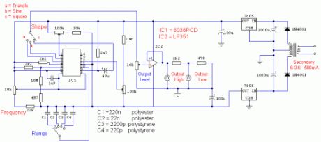
Built around a single 8038 waveform generator IC, this circuit produces sine, square or triangle waves from 20Hz to 200kHz in four switched ranges. There are both high and low level outputs which may be adjusted with the level control. This project makes a useful addition to any hobbyists workbench as well.Allof the waveform generation is produced by IC1. This versatile IC even has a sweep input, but is not used in this circuit. The IC contains an internal squarewave oscillator, the frequency of which is controlled by timing capacitors C1 - C4 and the 10k potentiometer. The tolerance of the capacitors should be 10% or better for stability. The squarewave is differentiated to produce a triangular wave, which in turn is shaped to produce a sine wave. All this is done internally, with a minimum of external components. The purity of the sine wave is adjusted by the two 100k preset resistors.The wave shape switch is a single pole 3 way rotary switch, the wiper arm selects the wave shape and is connected to a 10k potentiometer which controls the amplitude of all waveforms. IC2 is an LF351 op-amp wired as a standard direct coupled non-inverting buffer, providing isolation between the waveform generator, and also increasing output current. The 2.2k and 47 ohm resistors form the output attenuator. At the high output, the maximum amplitude is about 8V pk-pk with the square wave. The maximum for the triangle and sine waves is around 6V and 4V respectively. The low amplitude controls is useful for testing amplifiers, as amplitudes of 20mV and 50mV are easily achievable. (View)
View full Circuit Diagram | Comments | Reading(1622)
Sample Power Supply 2
Published:2013/7/23 21:15:00 Author:muriel | Keyword: Sample Power Supply
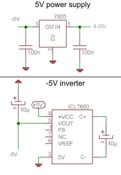
View full Circuit Diagram | Comments | Reading(928)
Sample Power supply 1
Published:2013/7/23 21:15:00 Author:muriel | Keyword: Sample Power supply
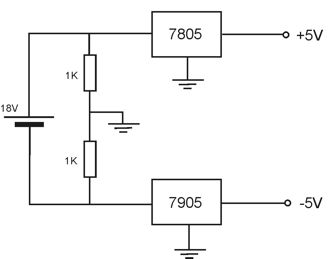
View full Circuit Diagram | Comments | Reading(2185)
TTL Power Supply
Published:2013/7/18 20:52:00 Author:muriel | Keyword: TTL , Power Supply
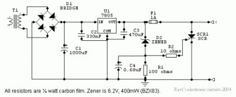
Power supplies that are intended to be used with TTL logic circuitry must guard against over-voltage, which can destroy TTL chips very rapidly. The duration of over-voltage that can destroy TTL chips is much too brief to trigger any conventional fuse, so that only other semiconductor circuits can play any useful part in protecting a circuit against the type of failure of a stabilizer that leads to excessive voltage. As it happens, this is the most common type of stabilizer failure, so that the protection is necessary for any TTL circuit of any significance. Many modern digital circuits make extensive use of MOS devices, which are less susceptible to damage from over-voltage, but it is unusual to find a large digital circuit, which does not contain at least one or more TTL devices.In the circuit shown below, if the voltage at the output terminals rises above 6.2V, zener conducts charging capacitor C4. This voltage will fire the silicon-controlled rectifier (SCR), which quickly shorts-or puts a ‘crowbar’ – across the supply rails blowing the fuse.
Circuit DescriptionThe regulator IC is the familiar fixed voltage type such as LM7805. The 7805 is a three-pin regulator which requires a minimum voltage input of 7.5V to sustain stabilization, which an absolute maximum input voltage of 35V. The maximum load current is 1A and the regulation against input changes is typically 3-7mV for a variation of input between 7.1V and 25V. The regulation against load changes is of the order of 10mV for a change between 5mV and 1.5A load current. The noise voltage in the band from 10Hz to 100KHz is 40-50uV, and the ripple rejection is around 70db. Maximum junction temperature is 215 degrees C, and the thermal resistance from junction to case is 5 degrees C/W. This stabilizer is used extensively for power supplies in digital equipments.In the circuit, the capacitors that are shown connected each side of the IC are very important for suppressing oscillations and must not be omitted. In particular, the 330nF capacitor at the input must be wired across the shortest possible path at the pins of the IC.I chose a TIC 106A SCR because it can handle an anode current up to 4A at 100V, but has a very sensitive gate requiring only about 200uA to fire it. The SCR is only ‘on’ for a very short time and thus does not need a heat sink. If you use another type, it is not likely to display the same characteristics. Most SCR’s with a heavy anode current rating have insensitive gates. SCR’s with a lower anode current rating will need a heat sink.The rating of fuse depends on the power supply you are using the circuit with. Assuming a maximum power supply output current of about 200 to 300 mA, you can fit a 500mA fuse.The voltage at which the SCR switches on is largely dependent on the value of the zener. You can experiment with different values of zeners to protect other types of circuits. The 4000 series CMOS ICs have supply voltage limits of 15V (AE suffix) or 20V (BE suffix) and crowbar protection can be used for these too.
(View)
View full Circuit Diagram | Comments | Reading(1343)
Dual Regulated Power Supply
Published:2013/7/18 20:48:00 Author:muriel | Keyword: Dual Regulated, Power Supply
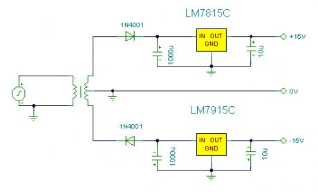
Notes:In this circuit, the 7815 regulatates the positive supply, and the 7915 regulates the negative supply. The transformer should have a primary rating of 240/220 volts for europe, or 120 volts for North America. The centre tapped secondary coil should be rated about 18 volts at 1 amp or higher, allowing for losses in the regulator. An application for this type of circuit would be for a small regulated bench power supply. (View)
View full Circuit Diagram | Comments | Reading(1102)
Batteries charger & PSU
Published:2013/7/18 20:34:00 Author:muriel | Keyword: Batteries charger & PSU
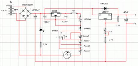
This circuit was created for digital cameras. It's known the digital cameras have considerable power consumption. For example my camera Minolta E223 requires approximately 800 mA. In practice a mains power supply or high capacity NiMH accumulators (batteries) can satisfy this demand.
This circuit consists of two parts, charger and adapter. The transformer, rectifier bridge and buffer condensator are common. Adapter is quite simply its main part is an adjustable voltage regulator LM 317 according to usual setting. Output is a suitable for camera jack plug. Voltage can be adjusted in range 2-9 V.In the charger circuit a 7805 fixed voltage regulator works as current generator assured constant current during charging. This charging current can be adjusted with the 100 /1W potentiometer in range about 50-300 mA indicated by a small current measuring instrument. From one to four batteries can be charged simultaneously. The switch must be set according to number of batteries, and charging current of batteries given by manufacturer must be adjusted. This circuit doesn't measure charging time and charging condition of batteries. Manufacturers give charging time, usually 14-16 h. I solved this problem with a simply, cheap mechanical mains timer. I think its accuracy is sufficient.
(View)
View full Circuit Diagram | Comments | Reading(1153)
Discharger for Receiver Battery Packs
Published:2013/7/18 20:33:00 Author:muriel | Keyword: Discharger , Receiver, Battery Packs
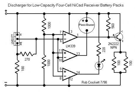
View full Circuit Diagram | Comments | Reading(977)
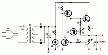
Nicad Battery Charger 2
Published:2013/7/17 22:01:00 Author:muriel | Keyword: Nicad Battery Charger
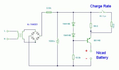
Notes:This simple charger uses a single transistor as a constant current source. The voltage across the pair of 1N4148 diodes biases the base of the BD140 medium power transistor. The base - emitter voltage of the transistor and the forward voltage drop across the diodes are relatively stable. The charging current is approximately 15mA or 45mA with the switch closed. This suits most 1.5V and 9V rechargeable batteries. The transformer should have a secondary rating of 12V ac at 0.5amp, the primary should be 220/240volts for Europe or 120volts ac for North America. (View)
View full Circuit Diagram | Comments | Reading(1248)
Ni -Cd Batteries Charger
Published:2013/7/17 22:00:00 Author:muriel | Keyword: Ni -Cd Batteries Charger
View full Circuit Diagram | Comments | Reading(1140)
10 Amp 13.8 Volt Power Supply
Published:2013/7/17 21:58:00 Author:muriel | Keyword: 10 Amp , 13.8 Volt, Power Supply
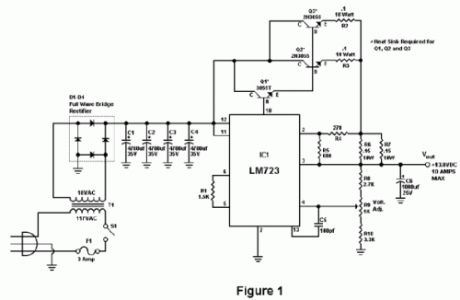
View full Circuit Diagram | Comments | Reading(1481)
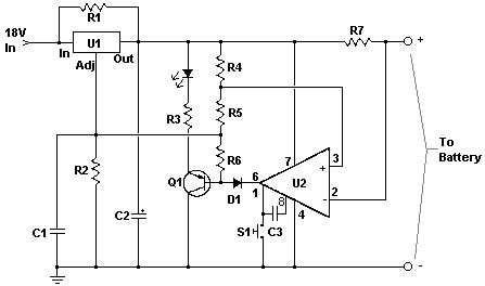
0-50V 2A Bench power supply
Published:2013/7/17 21:57:00 Author:muriel | Keyword: 0-50V , 2A, Bench power supply
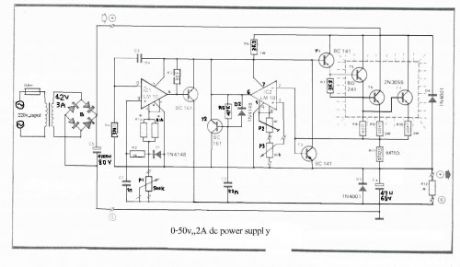
I use the lm10 IC because it has a reference voltage and that’s useful for dc power supply. With two ICs can take different output voltage and amperage. This circuit is protected from short circuit.P2 is for controlling the current at the range of 0-2A. Stabilize the output voltage with R4 on negative pin on op-amp and with R2 & P1 on positive pin.
Op-amp output controls T1 that not let ripple of voltage.T1 increase or decrease ampere of R6 and control the voltage of T5 & T4. Pin 1 is the reference voltage and reference voltage is losing some voltage on R1 that has 100uA . This current passes through P1 too.Vlose p1=100uA*Rp1This lose voltage regulate output voltage rate of output current is compare between reference voltage of P3 and lose voltage on R11.T3 is protecting short circuit with R11. For reduce out put voltage to 0v should parallel one resistor 470 ohm in out put. Minimum voltage is 0.4v. The maximum output voltage is fixed with R1b and should not become over of 50v. Therefore your transformer should give 36V, 3A with 4700uF capacitor. T6, T5, T7 need heatsilk. (View)
View full Circuit Diagram | Comments | Reading(1591)
LM317 VARIABLE POWER SUPPLY
Published:2013/7/17 21:56:00 Author:muriel | Keyword: LM317 , VARIABLE POWER SUPPLY
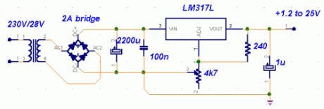
A truly timeless circuit. LM317 is a versatile and highly efficient 1.2-37V voltage regulator that can provide up to 1.5A of current with a large heat sink. It's ideal for just about any application. This was my first workbench power supply and I still use it.Since LM317 is protected against short-circuit, no fuse is necessary. Thanks to automatic thermal shutdown, it will turn off if heating excessively. All in all, a very powerful (and affordable!) package, indeed.Although LM317 is capable of delivering up to 37V, the circuit pictured here is limited to 25V for the sake of safety and simplicity. Any higher output voltage would require additional components and a larger heat sink.Make sure that the input voltage is at least a couple of Volts higher than the desired output. It's ok to use a trimmer if you're building a fixed-voltage supply.
Possible uses:Variable workbench power supply, fixed-voltage supply... Just about any possible application when no more than 1.5A is necessary.
(View)
View full Circuit Diagram | Comments | Reading(1278)
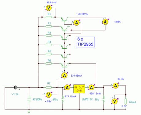
12 Volt 30 Amp PSU 2
Published:2013/7/17 21:55:00 Author:muriel | Keyword: 12 Volt, 30 Amp , PSU
View full Circuit Diagram | Comments | Reading(1212)
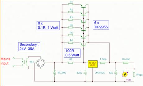
12 Volt 30 Amp PSU
Published:2013/7/17 21:54:00 Author:muriel | Keyword: 12 Volt, 30 Amp, PSU
View full Circuit Diagram | Comments | Reading(1174)
Transformerless Power Supply 2
Published:2013/7/17 21:52:00 Author:muriel | Keyword: Transformerless Power Supply
View full Circuit Diagram | Comments | Reading(1117)
DC Power Supply
Published:2013/7/17 21:50:00 Author:muriel | Keyword: DC Power Supply
View full Circuit Diagram | Comments | Reading(0)
Car Battery Charger 2
Published:2013/7/17 21:49:00 Author:muriel | Keyword: Car Battery Charger
This charger will quickly and easily charge most any lead acid battery. The charger delivers full current until the current drawn by the battery falls to 150 mA. At this time, a lower voltage is applied to finish off and keep from over charging. When the battery is fully charged, the circuit switches off and lights a LED, telling you that the cycle has finished.
PartsR1 500 Ohm 1/4 W ResistorR2 3K 1/4 W ResistorR3 1K 1/4 W ResistorR4 15 Ohm 1/4 W ResistorR5 230 Ohm 1/4 W ResistorR6 15K 1/4 W ResistorR7 0.2 Ohm 10 W ResistorC1 0.1uF 25V Ceramic CapacitorC2 1uF 25V Electrolytic CapacitorC31000pF 25V Ceramic CapacitorD1 1N457 DiodeQ1 2N2905 PNP TransistorU1 LM350 RegulatorU2 LM301A Op AmpS1Normally Open Push Button SwitchMISC Wire, Board, Heatsink For U1, Case, Binding Posts or Alligator Clips For Output
Notes1. The circuit was meant to be powered by a power supply, which is why there is no transformer, rectifier, or filter capacitors on the schematic. There is no reason why you cannot add these.2. A heatsink will be needed for U1.3. To use the circuit, hook it up to a power supply/plug it in. Then, connect the battery to be charged to the output terminals. All you have to do now is push S1 (the Start switch), and wait for the circuit to finish.4. If you want to use the charger without having to provide an external power supply, use the following circuit. (View)
View full Circuit Diagram | Comments | Reading(1061)
| Pages:16/291 1234567891011121314151617181920Under 20 |
Circuit Categories
power supply circuit
Amplifier Circuit
Basic Circuit
LED and Light Circuit
Sensor Circuit
Signal Processing
Electrical Equipment Circuit
Control Circuit
Remote Control Circuit
A/D-D/A Converter Circuit
Audio Circuit
Measuring and Test Circuit
Communication Circuit
Computer-Related Circuit
555 Circuit
Automotive Circuit
Repairing Circuit