
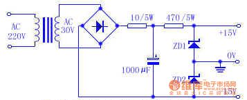
power supply circuit
Index
The TDA MCU power supply (A4) circuit diagram
Published:2014/4/24 21:04:00 Author:lynne | Keyword: The TDA MCU power supply (A4) circuit diagram
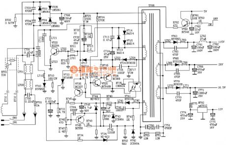
The TDA MCU power supply (A4) circuit diagram shown as follow:
(View)
View full Circuit Diagram | Comments | Reading(12461)
SONY G3F-K power circuit diagram
Published:2014/4/23 20:18:00 Author:lynne | Keyword: SONY G3F-K power circuit diagram, SONY G3F-K
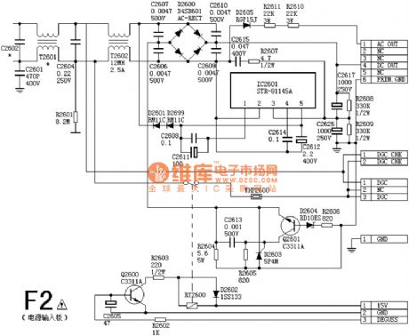
SONY G3F-K power circuit diagram shown as follow:
(View)
View full Circuit Diagram | Comments | Reading(5543)
Power supply circuit diagrams
Published:2014/4/17 21:32:00 Author:lynne | Keyword: Power supply circuit diagrams
Power supply circuit diagram shown as follow:
(View)
View full Circuit Diagram | Comments | Reading(6509)
Promote access power load high-current of a NAND gate circuit diagram
Published:2014/4/9 21:19:00 Author:lynne | Keyword: Promote access power load high-current of a NAND gate circuit diagram
Promote access power load high-current of a NAND gate circuit diagram as shown:
(View)
View full Circuit Diagram | Comments | Reading(2671)
Voltage-regulator diode threshold gate circuit diagram
Published:2014/4/7 21:37:00 Author:lynne | Keyword: Voltage-regulator diode threshold gate circuit diagram
Voltage-regulator diode threshold gate circuit diagram shown as follow:
(View)
View full Circuit Diagram | Comments | Reading(2685)
The thyristor ac voltage regulation circuit diagram
Published:2014/4/1 21:19:00 Author:lynne | Keyword: The thyristor ac voltage regulation circuit diagram
In order to stabilize the circuit diagram lamp brightness L, using thyristor AC automatic voltage regulator is the way, for access thyristor T5 on a diagonal line from the bridge of exchanges. Their trigger pulse generated by a single-junction transistor VT4. Transistor VT1 . VT2 and VT3 phototransistor play the role of the equivalent resistance when the lamp light due to supply voltage change, the change in resistance phototransistor, single-junction transistor control voltage phase also changed, so that the trigger pulse phase thyristor move, increase or decrease the thyristor time, the voltage on the approximation of L remains unchanged. brightness of the projector lamp is also approximately unchanged. makes light stability. The AC thyristor regulator circuit diagram shown in Fig.
(View)
View full Circuit Diagram | Comments | Reading(4126)
Made of 5 ma PNP transistor constant current source bridge type pressure sensor power supply circuit principle diagram
Published:2014/3/27 21:26:00 Author:lynne | Keyword: Made of 5 ma PNP transistor constant current source bridge type pressure sensor power supply circuit principle diagram
Made of 5 ma PNP transistor constant current source bridge type pressure sensor power supply circuit principle diagram shown as follow:
(View)
View full Circuit Diagram | Comments | Reading(3618)
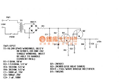
One-touch switching power supply circuit
Published:2014/3/27 21:24:00 Author:lynne | Keyword: One-touch switching power supply circuit
This circuit can be applied to a wide range of voltages (4.5V ~ 40V, the maximum current of 19A ), R5 is optional , when the input voltage is less than 20V can be short-circuited ; greater than the input voltage by connecting the 20V, R5 values R1 should meet with the partial pressure of the MOS GS voltage of V1 is less than greater than -20V -5V ( V2 when conduction ) as possible, the voltage V1 at the GS between ~-20V -10V so that a large current output V1 .Before the button is pressed , GS voltage V2 (ie C1 voltage ) is zero , V2 deadline , V1 , GS voltage is 0, V1 cut no output ; When you press S1, C1 charging , V2 GS voltage rises to about 3V when V2 guide pass and quickly saturated , V1 GS voltage is less than -4V, V1 saturated conduction , Vout with output, LED light ( and you should release the button ) C1 through R2, R3 continue to charge , V1, V2 state is locked ; when pressed again The next button , because V2 is saturated conduction state, the drain voltage of approximately 0V, C1 discharges through R3 , when put to approximately 3V , V2 deadline , V1 gate-source voltage is greater than -4V, V1 cut , Vout no output , LED tube off ( release button ), C1 through R2, R3 , and continues to be discharged outside of the circuit , V1, V2 to maintain the off state.Note : S1 makes Vout should be open or closed after the button is released , or will form the switching oscillation.One-touch switching power supply circuit shown in Fig.
(View)
View full Circuit Diagram | Comments | Reading(5370)
Single power supply switch plus or minus power circuit diagram
Published:2014/3/27 21:23:00 Author:lynne | Keyword: Single power supply switch plus or minus power circuit diagram, CD4069
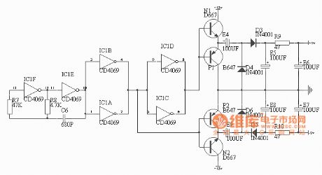
General Electric sound work, the need to provide positive and negative power. But in cars, boats, trains and other vehicles can only use battery power, a power supply circuit here, we want to help. The power from the oscillator circuit, inverter, rectifier and pusher and components such as filters, the circuit works as shown
Oscillator
This is a typical CMOS gate by (CD4069) constitute oscillator. Shock accuracy of 10-2 to 10-3, the shock process is as follows: Let the circuit at a time point B is high then the AB point to charge the capacitor through a resistor R8. The beginning of charging, the voltage across the capacitor is not due mutation, making the C point mutation to high potential, with the charge of conduct, C point potential gradually decreased. When the C-point conversion potential is lower than the voltage CMOS NAND gate, NAND gate 41F flip, A point goes high, B point becomes low. Since the voltage across the capacitor is not mutated, making the C point mutation to low potential. A point to the capacitor through a resistor R8 C6 reverse charge. With the charge carried, C point potential gradually increased when the C-point potential is higher than the conversion voltage CMOS NAND gate, NAND gate 41F flip, A point goes low, B point is to charge the capacitor through a resistor R8 C6 ...... repeating the above procedure, the formation of oscillation, the output pulse voltage at the point B. This oscillation frequency is f = 1/2ΠR8C6 = 1/2 * 3.14 * 4.7 * 103 * 680 * 10-12 = 49.8KHz, duty cycle 2. Figure resistor R7 (47K) Average value of R7 = (5 ~ 10) R8, its role is twofold: 1) to reduce the impact of power supply variations on the oscillation frequency. 2) reduce dynamic power circuits work.
Inverters
Divided into two groups of four inverters, respectively, opposite phase output pulse voltage, which pairwise parallel to increase the output current (SLR maximum output current of 1.5 mA, the shunt can output 3 mA). Advantages of CMOS inverters are: anti-interference ability, wide supply voltage range (3 ~ 20V), just apply to this circuit, the power of the circuit is 18V.
Pusher
Look at the two transistors N1 and P1 works, N1 consisting of common collector amplifier circuit for amplifying the input pulse voltage signal positive half cycle; P1 is also composed of common collector amplifier circuit for amplifying the negative half cycle of the input pulse voltage signal, they synthesized output phase with the input signal phase at point E, but opposite current amplification (up to two or three times) pulse voltage signal. Two transistors N2 and P2 with the working principle is similar, but the phase of the pulse signal and the voltage signal output from the point E to point F in opposite output, a rectifying circuit for the following positive and negative voltages, respectively, the entire effluent. In this circuit, the two transistors selection D647, D667, its argument is: 0.9w, +1 A/-1A.
Rectifier and filter
This part of the circuit is very classic, although voltage doubling rectifier circuit, but the loss due to other reasons, in this circuit when the load is +12 V/-12V, rated load +9 V/-9V. This power supply circuit provides power less than 11W.
Further, in the practical application of the circuit, the oscillation signal of the presence of 50KHZ, note frequency shielding, such as a printed board with this part of the circuit enclosed foil shielding. In addition, the power supply ripple factor depending on the desired single-supply ripple. Since the commissioning of the project power is not available, so long as the part is good, the connection is correct, it can work properly.
Single power converter shown in Figure positive and negative power supply circuit
(View)
View full Circuit Diagram | Comments | Reading(5541)
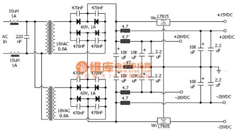
Dual polarity power supply circuit diagram
Published:2014/3/27 21:21:00 Author:lynne | Keyword: Dual polarity power supply circuit diagram,
Dual polarity power supply circuit diagram as shown:
(View)
View full Circuit Diagram | Comments | Reading(4708)
Several commonly used backup power supply circuit diagram
Published:2014/3/27 21:20:00 Author:lynne | Keyword: Several commonly used backup power supply circuit diagram, MC34164, LM2931T, ICL7673, MAX610, LM2935
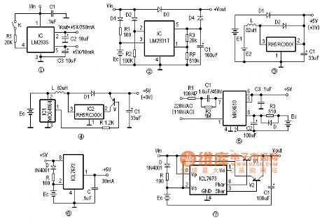
Here are a few dedicated uninterruptible power supply circuit, especially for low-power or batteries places. Can be used as a backup power source other low-voltage power circuit memory, microprocessors, CMOS circuits, timer and calendar clock circuit.
Self-based backup regulator
LM2935 is a low drop voltage regulator, in addition to a +5 V/750mA regulated output, the internal device also has a low quiescent backup regulator, its normal output is +5 V/10mA, Figure 1 shows a typical wiring LM2935 Figure. Backup function mainly regulator in the line when subjected to transient shocks (such as line input suddenly reaches 60V voltage exceeds the maximum input voltage transient limit), 750mA regulator output will automatically shut down to protect the internal circuitry and load, but still normal backup regulator output, as long as the reset level and ultra-low input voltage does not occur simultaneously, it can make a backup storage without data loss of normal power supply.
Power failure backup regulator circuit
Although low dropout regulator LM2931T just a battery regulator, using it as a power failure backup is very convenient. The circuit in Figure 2 when the normal power supply, input output directly through D3, D1 and R1 also by Ec backup battery trickle charge, LM2931T is high and 2 feet off the output; When the line when the input power failure, LM2931T 2 feet will be low, the output power to the load through D4 continued regulation. Backup circuit can accommodate a wide range of voltages, power regulator RP obtain suitable output circuit for the isolation diodes D1-D4, the best selection of low drop Schottky diode.
Backup power boost switch IC
RH5RCXXX series circuit is a three-terminal regulator IC CMOS switch, low current consumption of only 7.5uA. As long as the input voltage is greater than 0.9V, the boost switch output can be achieved, the conversion efficiency is generally above 80%. The circuit in Figure 3 constitutes a use RH5RCXX clamp boost backup power. The main power supply circuit E1, E2 as an auxiliary power when the main power output strong, diode D2 deadline, RH5RCXX boost circuit does not work; When the main power is turned down to D2, E2 will D1 auxiliary power off switch boost Backup power output circuit. Figure 4 is a power-saving backup power circuit. At higher battery voltage, output voltage detector 1 foot MC34164 blocking, V cutoff, power Ec directly through L, D1 output; supply Ec voltage drop is detected when IC1 effective, a pin output low, the end of the suction current of about 6mA, it was R so that V conduction, allowing the boost switch circuit, the battery Ec may continue to be used.
Transformerless power backup
With MAX's electricity converter MAX610 can constitute a +5 V uninterruptible power supplies, backup batteries use ultracapacitors. Under normal circumstances 2,8 feet rectified output of the IC through R3 backup battery trickle charge current is selected as the best one-tenth or less of battery capacity. When power cut, D conduction, so Ec by internal series regulator IC output freewheeling, the maximum output current up to 150mA, to ensure that the load is not power-down operation. It is noteworthy that the best choice of diode Schottky diode D, such as D83004, etc., buck capacitor C2 should have a withstand voltage of 450V or more, when the electricity is when 220V/50Hz, R1 take 100 ohms; When the mains voltage is When 110V/60Hz, R1 taken 47 ohm.
ASIC backup power
ICL7673 is a monolithic CMOS ASIC-based backup power can achieve output 2.5-15V input voltage range of backup power, then the normal power supply pin Vp, Vs take a backup power supply, power supply was normal Pbar bottom level, and Sbar blocking ; when energized,, Pbar blocked, and Sbar bottom level output; supply of +5 V when the output current is 38mA, when the power supply 3V, the output current is 30mA, Sbar and Pbar end load capacity of about 50mA. Small power backup power supply 6 is constituted by the ICL7673, spare battery with 3.6V lithium battery or super capacitor bank. When normal power supply, battery trickle charge to get. +5 V power failure, +3.6 V output will freewheeling diode D prevents backflow backup battery power is consumed in the normal end; To accommodate large load backup ICL7673, and Figure 7 pipe expansion flow output by PNP, V1 under normal circumstances lead Tong, V2 at the time of the backup power supply is turned on.
Several commonly used backup power supply circuit shown in Figure
(View)
View full Circuit Diagram | Comments | Reading(4950)
Voltage frequency conversion composed MPX2100 circuit diagram
Published:2014/3/25 21:33:00 Author:lynne | Keyword: Voltage frequency conversion composed MPX2100 circuit diagram, MPX2100
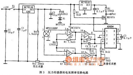
Voltage frequency conversion power
Figure is constituted by the voltage frequency conversion circuit MPX2100 . The circuit consists of a voltage amplification and frequency conversion of two parts, by a 4 op amp and a few resistors amplifier circuit , which has differential mode gain and high common-mode rejection ratio , and high input impedance, you can adjust the bias circuit. Differential amplifier circuit is mainly done by A1, A2 op amp feedback circuit is used to prevent the inflow of sensor negative side . At zero pressure, the difference between the voltage of the sensor between 2 feet and 4 feet to zero . If 2 feet and 4 feet each common-mode voltage 4V ( half the supply voltage sensor ), the A1 is a pin voltage is also 4V, so that the voltage through the A3 and A4 road to its output voltage is zero pressure . Zero pressure offset introduced by the output of R4 and R12, R12 can be set to adjust the bias voltage. By R7 choose from 13 feet to see past impedance , typically 1kΩ. Amplifier gain AV = R5 [1 + (R11/R10)] / R6 = 125. Select a gain of 125 allows the sensor full scale output swing amplified when 32mV to 4V swing .A3 output terminal voltage of 0.5 ~ 4.5V after by V / F conversion to the output frequency 1 ~ 10kHz . A3 8 feet and AD654V / F converter is connected . Its full- scale output frequency is determined by R3, R13 and C3, and can be calculated according to the following formula :Fout ( Full Scale ) = Vin / [10 (R3 + R15) C3] (View)
View full Circuit Diagram | Comments | Reading(2724)
Low loss power supply of solar-powered light circuit diagram
Published:2014/3/20 21:02:00 Author:lynne | Keyword: Low loss power supply of solar-powered light circuit diagram, LM324, LM385
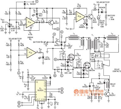
Solar lamp circuit is a low-loss circuit, using a four-pin 7W CFL (compact fluorescent lamps) and a 12V ,7-Ahr sealed maintenance-free batteries. Inverter efficiency greater than 85%, the quiescent current is less than 2mA. It has a protective function with battery discharge and overcharge protection feature parallel charge controller. Low quiescent current, over-discharge protection function and overcharge protection to ensure that the three very long battery life. Preheat function prevents the inverter CFL ends of black, thus extending its life. This circuit can be used as a reliable and compact portable light source in rural areas, in urban use as emergency light systems. Shunt charge controller circuit comprises IC1 (low current 2.5V voltage reference LM385) and IC2 (LM324 comparator). With resistors R1 ~ R8 and transistor Q1 IC2A prevent battery discharge. Solar-powered lights low-loss circuit diagram shown in Figure:
(View)
View full Circuit Diagram | Comments | Reading(5079)
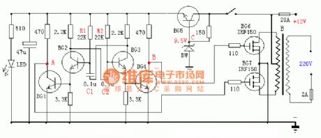
A3 (A4) power supply circuit
Published:2014/3/19 21:15:00 Author:lynne | Keyword: A3 (A4) power supply circuit, A3 (A4)
A3 (A4) power supply circuit shown as follow:
(View)
View full Circuit Diagram | Comments | Reading(4387)
SONY G3FK2 power circuit diagram
Published:2014/3/19 21:14:00 Author:lynne | Keyword: SONY G3FK2 power circuit diagram, G3FK2
SONY G3FK2 power circuit diagram shown as follow: (View)
View full Circuit Diagram | Comments | Reading(2852)
Enter 1.5 V to 22.5 V output circuit principle diagram
Published:2014/3/19 21:12:00 Author:lynne | Keyword: Enter 1.5 V to 22.5 V output circuit principle diagram,
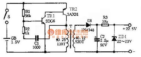
As shown is an output voltage 22.5V DC side of the booster circuit that can be used instead of 22.5V DC battery, which use a multimeter in a 1.5V battery-powered operating current of 25mA output current is about 0.5mA high barrier for Multimeter wealthy enough. circuit composed of complementary multivibrator TR1 and TR2, its oscillation frequency is approximately 2KHz.T is the primary line of step-up transformer load up multivibrator secondary liters a high voltage output voltage of the pulse wave which the voltage after the rectifier diode D1 and the capacitor C2 becomes wave DC high voltage, and then after the resistor R3 and the voltage regulator tube ZD1 can output a stable high voltage.
(View)
View full Circuit Diagram | Comments | Reading(5835)
Inverter power supply circuit diagram
Published:2014/3/18 21:19:00 Author:lynne | Keyword: Inverter power supply circuit diagram,
Inverter power supply circuit diagram shown as follow:
(View)
View full Circuit Diagram | Comments | Reading(5083)
Switching power supply circuit diagram
Published:2014/3/18 21:19:00 Author:lynne | Keyword: Switching power supply circuit diagram
Switching power supply circuit diagram as shown:
(View)
View full Circuit Diagram | Comments | Reading(3508)
RC Buck power supply circuit
Published:2014/3/17 21:38:00 Author:lynne | Keyword: RC Buck power supply circuit,
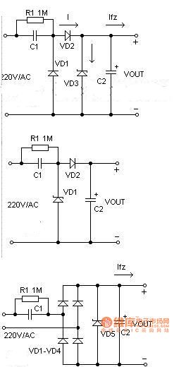
Conventional methods AC power is converted to low voltage DC rectifier filter before using the step-down transformer, when restrictions on the size and cost factors, the most simple and practical method is to use capacitor step-down power supply.
First, the circuit schematic
Simple basic buck power supply circuit capacitance in Fig, C1 is a step-down capacitor, D2 for the half-wave rectifier diode, D1 in the negative half cycle of the mains to provide a discharge circuit C1, D3 is a Zener diode, R1 is power off After the charge C1 bleeder resistor. Is often used in practical applications of the circuit shown in Figure 2. When the need to provide a larger load current, the bridge rectifier circuit can be used as shown in Figure 3.
Unregulated rectified DC voltage is generally higher than 30 volts, and will vary with changes in load current large fluctuations occur, it is because a lot of the reason of such power due to internal resistance, it is not suitable for high current power supply applications.
Conventional methods AC power is converted to low voltage DC rectifier filter before using the step-down transformer, when restrictions on the size and cost factors, the most simple and practical method is to use capacitor step-down power supply.
First, the circuit schematic
Simple basic buck power supply circuit capacitance in Figure 1, C1 is a step-down capacitor, D2 for the half-wave rectifier diode, D1 in the negative half cycle of the mains to provide a discharge circuit C1, D3 is a Zener diode, R1 is off C1 charge after power bleeder resistors. Is often used in practical applications of the circuit shown in Figure 2. When the need to provide a larger load current, the bridge rectifier circuit can be used.
Unregulated rectified DC voltage is generally higher than 30 volts, and will vary with changes in load current large fluctuations occur, it is because a lot of the reason of such power due to internal resistance, it is not suitable for high current power supply applications.
Second, the device selection
1 circuit design, the exact value should be measured load current, and then select the reference sample capacity buck capacitor. Because the capacitor C1 through the buck to the load current Io, flowing C1 actually charge and discharge current Ic. C1 greater capacity, the smaller the capacitive reactance Xc, then flows through C1 charge and discharge current increases. When the load current Io is less than C1 charge and discharge current, the excess current will flow through the regulator, if the regulator is less than the maximum allowable current Idmax Ic-Io when the regulator could easily lead to burnout.
(2) To ensure reliable operation of C1, the pressure should be chosen to be greater than twice the supply voltage.
3 bleeder resistor R1 must be selected to ensure that within the required time exhausting the charge on C1.
Third, the design example
Known C1 is 0.33μF, AC input 220V/50Hz, seeking circuit can supply a maximum current load. C1 reactance Xc in the circuit is:
Xc = 1 / (2 πf C) = 1 / (2 * 3.14 * 50 * 0.33 * 10-6) = 9.65K
Flows through the capacitor C1 of the charging current (Ic) is:
Ic = U / Xc = 220 / 9.65 = 22mA.
Capacitor C1 is often the relationship between blood pressure and the load current Io capacitance C can be approximated that: C = 14.5 I, where C is the capacity of the unit is μF, Io unit is A. Capacitor Buck is a non-isolated power supply, pay special attention to the application of isolation, to prevent electric shock.
RC Buck power supply circuit shown in Fig. :
(View)
View full Circuit Diagram | Comments | Reading(4586)
High power regulator inverter circuit diagrams
Published:2014/3/17 21:22:00 Author:lynne | Keyword: High power regulator inverter circuit diagrams, TL494, 2SK906, 2SK564
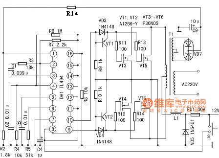
The use of the composition of 400W power regulator TL494 inverter circuit. It excited transform part is TL494, VT1, VT2, VD3, VD4 constitutes a sink current drive circuit, driving two of each two 60V/30A MOS FET switch. For increasing the output power of each channel can be three to four switches in parallel applications, the circuit unchanged. The inverter TL494 application as follows:
1,2 feet constituted regulator sampling error amplification system, a positive input pin input sampling secondary winding rectifier inverter output 15V DC voltage, the R1, R2 partial pressure, so that the first leg of the inverter Nearly 4.7 ~ 5.6V voltage sampling work. Inverting input pin 2 Input 5V reference voltage (from 14 feet out). When the output voltage is reduced, a lower pin voltage error amplifier output low, the PWM circuit output voltage increases. When a voltage is normal foot 5.4V, 2-pin voltage is 5V, 3-pin voltage is 0.06V. Then the output AC voltage is 235V (square-wave voltage). 4-pin external R6, R4, C2 set the dead time. Normal voltage is 0.01V. 5,6 pin external CT, RT triangle wave oscillator frequency is set to 100Hz. 5 pin voltage is normal 1.75V, 6-pin voltage is 3.73V. 7 feet for common ground. 8, 11 feet inside the drive output transistor collector, 12 feet for the TL494 pre-supply terminal, this three-terminal controlled by a switch S TL494 start / stop, as the inverter control switch. When S1 is turned off, TL494 no output pulse, so the switch VT4 ~ VT6 no current. When S1 is turned on, this tripod is the battery voltage is positive voltage. 9,10 feet inside the driver stage transistor emitter output two different positive pulse timing. Normal voltage is 1.8V. The first 13, 14 feet 14 feet 5V reference voltage output, so that there is 5V 13 feet high, the control gates, flip-flop output two drive pulses, for push-pull switching circuits. The first 15-pin external 5V voltage, constitute the reference voltage error amplifier inverting input to the non-inverting input terminal 16 feet high protection constitute input. In this connection, when the input is greater than 16 feet high of 5V, the output voltage can be reduced through the role of regulator, on or off the drive pulses to achieve protection. In its excited inverter output is almost no possibility of overpressure, so the circuit is not used in the first 16 feet, the ground by a resistor R8.
The capacity of 400VA inverter with power frequency transformer cores using 45 × 60mm2 silicon steel. The primary winding of wire with a diameter of 1.2mm, two and around 2 × 20 turns. Secondary sampling using 0.41mm wire winding around the 36-turn, center tap. 230V secondary winding is calculated by using the 0.8mm enameled wire wound 400 turns. Switch VT4 ~ VT6 available 60V/30A any type of N-channel MOS FET tube instead. VD7 available 1N400X series ordinary diodes. The circuit is almost without debugging to work properly. When C9 positive terminal voltage is 12V, R1 can be between 3.6 ~ 4.7kΩ choice, or 10kΩ potentiometer is adjusted so that the output voltage rating. If this is the inverter output power increases almost 600W, the primary current in order to avoid excessive increase of the resistive losses, should the battery switch to 24V, VDS can be used to switch high current MOS FET 100V tube. It should be noted that the choice of multi-tube rather parallel, rather than choose single IDS greater than 50A of the switch, the reason is: a higher price, two driving too difficult. Suggested the use of 100V/32A of 2SK564, 2SK906 or optional three parallel applications. Meanwhile, the transformer core cross section required to achieve 50cm2, calculated by the ordinary power transformer turns and calculated diameter, or the use of alternative waste transformer UPS-600. Such as refrigerators, electric fans powered, do not forget to join LC low-pass filter.
Power regulator inverter circuit shown in Figure:
> (View)
View full Circuit Diagram | Comments | Reading(9261)
| Pages:1/291 1234567891011121314151617181920Under 20 |
Circuit Categories
power supply circuit
Amplifier Circuit
Basic Circuit
LED and Light Circuit
Sensor Circuit
Signal Processing
Electrical Equipment Circuit
Control Circuit
Remote Control Circuit
A/D-D/A Converter Circuit
Audio Circuit
Measuring and Test Circuit
Communication Circuit
Computer-Related Circuit
555 Circuit
Automotive Circuit
Repairing Circuit